
Global epoxy molding compound demand for semiconductor packaging reached USD 2,067 million in 2024 and is forecast to hit USD 3,635 million by 2030, equating to a 6.7% CAGR through 2032 on a value basis, while tonnage growth runs hotter at 8.2% CAGR to 1,104,779 tons by 2032 [S4].
Asia-Pacific absorbed 56.55% of 2024 EMC demand, anchored by China, Taiwan, South Korea, and Japan foundries, with Green (halogen-free) formulations already holding a 51.45% share of the type mix in the same year [S4].
What a Semiconductor-Grade EMC Actually Is
An EMC for IC packaging is a highly filled, electrically stable thermoset built on epoxy cresol novolac resin cured with a phenolic novolac hardener, accelerated and loaded with 80–90 wt% spherical silica in a multimodal particle distribution to control CTE, viscosity, and spiral flow [S2]. Beyond resin and filler, the formulation carries flame retardants, adhesion promoters, parting agents, carbon black pigment, and ionic-getter additives, with each supplier tuning the recipe for a specific package geometry and transfer-molding window [S2][S3].
Wafer thinning is the dominant design pressure on the material: single-wafer thickness dropped from 175 µm in the 1990s to 20 µm by 2024, and the IC transistor count passed 10 billion per die in 2020, both of which force EMC developers to lower modulus, raise Tg, and shrink filler cut to keep warpage and delamination under control [S5].
Selection Criteria That Matter on the Production Floor
For high-power discrete packages, HTRB (High Temperature Reverse Bias) survivability is the first gate, and modern EMCs targeting TO-220, TO-92, and fullpack power parts are graded for a glass transition above 200 °C, with the LINQSOL EMC-7560 cited at Tg 205 °C and an explicit HTRB pass claim [S1].
For BGA and LGA array packages, ultra-low moisture absorption and high fluidity are the gatekeepers, because delamination at the substrate interface is the dominant field-failure mode; products such as LINQSOL EMC-9012 and Hysol GR910-K are positioned for BGA/LGA with low stress and halogen-free W/S control respectively [S1].
For SOP, QFP, and SOT lines, spiral flow length, wire-sweep control, and cost-per-shot dominate, which is why grades like LINQSOL EMC-7142 (SOP/QFP), EMC-6043 (SOT/modules), and EMC-9131 (high spiral flow) sit in the catalog, while thermally conductive variants such as EMC-5013 add Al2O3 or similar fillers for TO/fullpack heat extraction [S1].
Process Window: Transfer, Compression, and Wafer-Level Molding
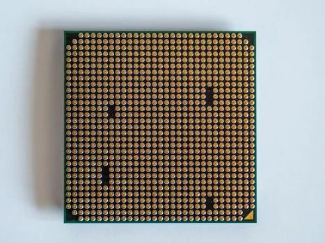
Three encapsulation routes coexist on the shop floor, and the 2025 review by Othman et al. lines them up against the same defect list of voids, warpage, and delamination: transfer molding for leadframe and standard QFN/BGA, compression molding for large-area and low-stress parts, and underfill or mold-underfill (MUF) for flip-chip and wafer-level packages, with MUF now common in fan-out wafer-level packaging (FOWLP) [S3].
Each route imposes a different rheology target: transfer molding needs long spiral flow to chase fine pitch without wire sweep, compression molding tolerates higher viscosity but punishes viscosity drift across the platen, and wafer-level molding demands filler sizes small enough to clear sub-100 µm gaps, which is why bimodal and trimodal silica PSDs have become the default in advanced EMC [S2][S3].
Supply and Sourcing Map for 2026
Concentration of EMC supply sits in North Asia: the major formulators (Hitachi Chemical/Henkel-adjacent Hysol, Sumitomo, Samsung SDI, and the LINQSOL/Resonac family) plus the captive lines run by the OSATs, with the global supplier list now counted at 25 named companies and a market modeled out to 2035 by multiple research houses [S6][S8][S9].
Raw-material volatility remains the binding constraint, not molding-press capacity, because epoxy resin, phenol novolac hardener, and spherical silica price swings translate directly into EMC price moves, and several suppliers are now qualifying bio-based and recyclable resin systems to hedge that exposure [S3][S4].
Comparison: Discrete-Power EMC vs Array-Package EMC vs Flip-Chip MUF
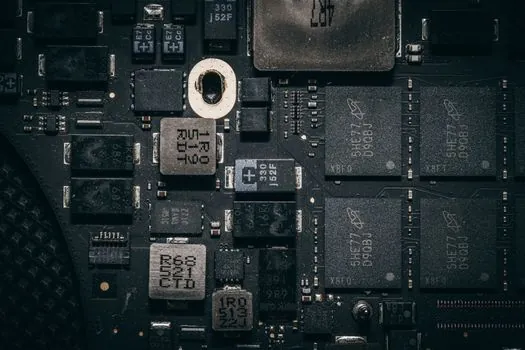
On a criteria basis, discrete-power EMCs (TO-220, fullpack, SOT) win on Tg (≥205 °C) and HTRB survival, lose on spiral-flow length and minimum filler cut; array-package EMCs (BGA, LGA, QFN) win on moisture absorption and low modulus, lose on thermal conductivity; flip-chip mold-underfill (MUF) EMCs win on gap-filling in fine-pitch stacks and compatibility with FOWLP, but lose on reworkability because the cure is irreversible and any underfill void becomes a yield-killer at reflow [S1][S3].
If the application is high-voltage automotive, a Tg above 200 °C and HTRB rating is the gate, with thermal conductivity a secondary axis; if the application is smartphone BGA or SiP, ultra-low moisture absorption and halogen-free compliance with RoHS are the gate, with Tg dropping to 150–170 °C; if the application is fan-out wafer-level, filler cut and MUF flow are the gate, with traditional Tg targets relaxing in favor of warpage control on 20 µm-thinned wafers [S1][S4][S5].
Standards, Reliability Tests, and Where the Formulators Are Headed
Reliability is enforced by JEDEC-style moisture sensitivity levels (MSL), HTRB, and temperature-cycling tests on the encapsulated part, while material compliance runs through RoHS, halogen-free (typically <900 ppm Cl, <900 ppm Br), and increasingly REACH substance tracking, all of which the Green EMC segment already meets across 51.45% of 2024 volume [S4].
Roadmap work across the supplier base is converging on three axes: higher thermal conductivity fillers (AlN, Al2O3, and hybrid boron nitride) to remove heat from stacked-die parts, lower-modulus resins with biphenyl or naphthalene backbones to keep warpage under control on thin wafers, and AI-driven molding process control to cut void and wire-sweep defects in real time, as flagged in the 2025–2026 review literature [S3][S5].
For sourcing teams, the practical 2026 spec to put on the RFQ is: Tg ≥150 °C for array packages, ≥200 °C for power discretes, ionic content and Cl/Br levels per JEDEC/RoHS, spiral-flow length matched to the mold chase, and an explicit MSL-3 or MSL-2 rating confirmed on the data sheet; packaging-line buyers chasing lead-time data can cross-reference the broader engineering plastic compound lead-time picture for October 2026, which sits in the same resin-and-filler supply pool [S1][S4]. Procurement of the supporting encapsulant packaging and logistics packaging for bagged EMC, and the packaging material used for moisture-barrier bags, also has to be locked in parallel, because the supply of the EMC drum and the supply of the EMC itself often ride the same resin upstream.
For the relevant spec sheets and selection criteria, see concrete curing compound.