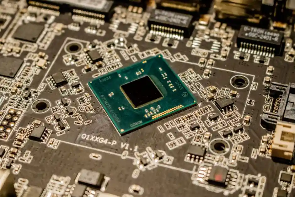
Electronics-grade solvent selection is governed by ionic contamination limits under 1 ppm chloride and under 0.1 ppm sodium, trace metal control to ppb levels via ICP-MS, and a residue-on-evaporation ceiling below 5 ppm, per glycol-ether-ester reference data published 2026-03-26 [S3].
These thresholds, not bulk purity alone, separate a true semiconductor or photoresist grade from a general industrial solvent. A 99% isopropyl alcohol (IPA) drum that is acceptable for degreasing will fail a wafer or display line on water content, ionic residue, or non-volatile residue; the same applies to acetone, ethyl acetate, NMP, DMF, DMSO, and THF when used beyond commodity cleaning [S1][S2].
Solvent Categories Matched to Electronics Process Steps
Electronics solvents split into four functional groups, each with distinct purity gates: photoresist solvents (EGMEA, EGEEA, EGMEMA glycol ether esters), PCB and contact cleaners (99%+ IPA plus no-clean flux removers), conformal-coating strippers, and encapsulation protection solvents for die attach and potting [S2][S3][S4].
Within each group, the same molecule can be qualified at different grades. IPA is supplied at 70% (30% water, unsuitable for critical cleaning), 99% (electronics-grade, low residue), and ESD-safe static-dissipative blends; acetone, NMP, and DMF have analogous electronic, semiconductor, and HPLC tiers [S1][S2]. The user's industrial solvent inventory should be tagged by grade, not just chemistry.
Purity Gates That Decide Acceptance or Rejection
Six parameters are non-negotiable for electronics acceptance: assay/purity, water content (Karl Fischer), acidity/alkalinity, APHA color, non-volatile residue, and trace metal or ionic impurity limits, with photoresist grades additionally specifying boiling range within ±1 °C and residue-on-evaporation under 5 ppm [S1][S3].
Semiconductor-grade solvents hold chloride under 1 ppm and sodium under 0.1 ppm to prevent electrochemical migration between conductors; trace metals (Fe, Cu, Al, Na, K) must be controlled to ppb levels by ICP-MS to avoid deep-level traps in the silicon band gap. Standard industrial-grade material does not meet these limits and cannot be substituted for wafer, photoresist, or display-panel steps [S3]. Buyers should request a lot-specific COA, SDS/MSDS, and TDS rather than a generic data sheet [S1].
EGMEA vs EGEEA vs EGMEMA: Glycol Ether Ester Comparison
EGMEA (ethylene glycol methyl ether acetate), EGEEA (ethylene glycol ethyl ether acetate), and EGMEMA (ethylene glycol methyl ether methacrylate) differ in evaporation rate, viscosity, and resist-polymer solvency, and the choice is set by the spin-coating or spray process window rather than raw solvency power [S3].
EGMEA is the workhorse for novolac and acrylic photoresist casting, with the fastest evaporation of the three. EGEEA offers a slower, more uniform drying profile, which is preferred for thicker films and display-panel coatings where ±5 nm film-thickness uniformity is required across a 200 mm wafer. EGMEMA is used where methacrylate reactivity is needed for specific resist systems or conformal-coating chemistries. All three are run at electronic or semiconductor grade with the same ionic and metallic limits listed above; selecting among them is a process-engineering decision, not a purity decision [S3].
PCB Cleaning, Flux Removal, and Contact Cleaning
For PCB surface cleaning, 99%+ electronics-grade IPA is the default; 70% IPA introduces ionic contamination and water spots and is rejected for any critical step. No-clean and polymerized rosin flux residues are not fully removed by standard IPA, so engineered flux removers from Chemtronics and Techspray are specified for those residues, with separate grades for rosin, no-clean, and water-soluble (OA) flux systems [S2].
Contact cleaners are a distinct chemistry class: zero residue, fast-evaporating, and formulated for connectors, sliding contacts, and potentiometers. ESD-safe variants are required for static-sensitive assemblies. Conformal coating removal is chemistry-matched to the coating: acrylic strips with standard solvents, urethane and epoxy require stronger chemistry and longer dwell times, and silicone typically requires mechanical abrasion [S2]. Engineers who treat these as interchangeable industrial solvent categories will see field leakage and dendritic growth, not just a clean visual. For housings and enclosure-related cleaning, a separate material line such as industrial adhesive is often paired with the solvent workflow to bond or re-seal after stripping.
Encapsulation, Potting, and Component Protection
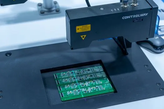
During encapsulation, any ionic or organic impurity introduced at the surface can compromise electrical performance, induce corrosion, or interfere with encapsulant adhesion, which is why high-purity solvent is specified for pre-potting surface preparation on semiconductors, sensors, and medical-device PCBs [S4].
Clean surfaces plus low residue translate directly into three measurable outcomes: reduced leakage current and electrochemical migration, maximized adhesion between the encapsulant (epoxy, silicone, urethane) and the device, and lower long-term contamination risk under thermal cycling. The selection rule is to match the solvent to the encapsulant chemistry; a solvent that swells or partially dissolves the housing polymer is disqualified regardless of its assay value [S4].
Packaging, Contamination Control, and Supplier Qualification
For electronics grades, container material and cleanliness, controlled-atmosphere filling and sealing, and pre-qualification sample packaging are as important as the certificate of analysis, because the solvent can be re-contaminated between the supplier's QC release and the point of use [S1].
Buyers should ask suppliers whether the standard product matches the electronics specification or whether a specialized grade must be arranged, and they should request COA, SDS/MSDS, and TDS for the actual lot. Drum, IBC, and specialty packaging options must be reviewed against the cleanroom or clean-zone transfer step; the wrong transfer fitting can negate the entire purity chain. A specification-first RFQ, including exact application, target spec, packaging, and order volume, returns more accurate quotes than a generic product name [S1].
Selection Criteria, Limitations, and When NOT to Substitute

Do not substitute a general industrial-grade solvent for any wafer, photoresist, or display-panel step, and do not use 70% IPA for critical PCB cleaning; both will fail ionic and residue limits and will drive yield loss rather than save cost. Standard IPA also cannot fully dissolve polymerized or no-clean flux, so a no-clean-compatible engineered remover is required where those fluxes are in use [S2][S3].
Conformal coating removal is the third high-risk substitution: assuming a single solvent will strip acrylic, urethane, epoxy, and silicone will at best give partial removal and at worst damage the PCB. The practical rule is to fix the substrate-coating-solvent triad before any production release and to lock the grade, not just the chemical name, into the purchase spec. For buyers scaling electronics-related enclosures and housings, parallel lines such as industrial camera module assembly use the same purity logic and benefit from a shared solvent-grade audit.
Trackable signals for the next sourcing cycle: tightened supplier disclosure of lot-level ICP-MS data for trace metals, the spread of 99%+ IPA and no-clean flux remover stocking in distribution, and any shift in glycol ether ester supply tied to display-panel capacity additions through 2026. These three data points are the most direct leading indicators of whether electronics-grade solvent availability is tightening or easing.
See also our earlier report, Lead Screw Selection Gates for Mining Duty: 2026 Spec Map.