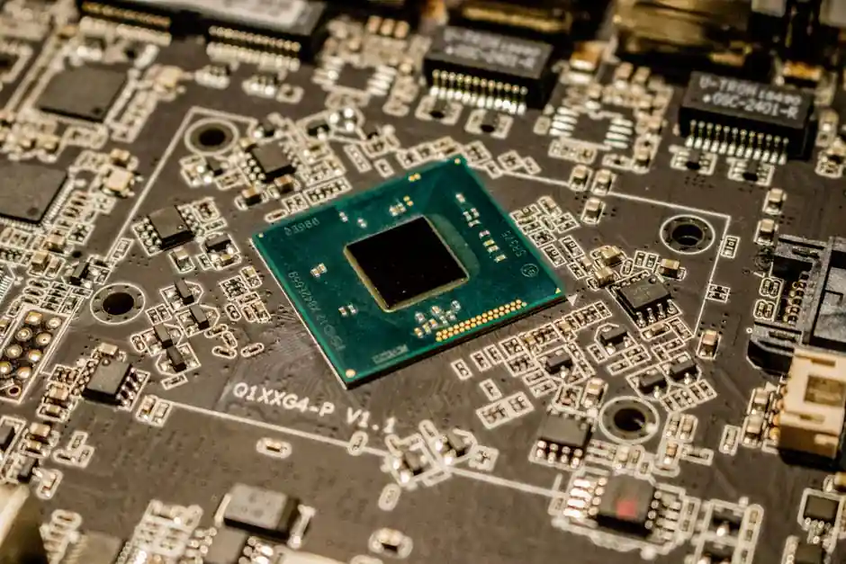
Ceramic substrates for power modules split cleanly along thermal conductivity: aluminum nitride (AlN) at 140–220 W/m·K versus dense alumina (96–99.5% purity) at roughly 20–30 W/m·K, and the choice is governed by die power density, current rating, and thermal-cycling exposure [S2][S4].
For high-voltage insulation, technical ceramics deliver dielectric strength of 10–20 kV/mm with volume resistivity above 10^14 Ω·cm, a combination metals and plastics cannot match simultaneously, which is why ceramic insulators, bushings, and standoffs are the default in transformers, switchgear, and power distribution hardware [S2].
Core Materials: Alumina, Aluminum Nitride, and Where Each Wins
Alumina (Al2O3) is the cost-effective baseline for lower-power modules and general-purpose insulators, with thermal conductivity in the 20–30 W/m·K band and dielectric strength above 20 kV/mm, supporting PCB operation at temperatures beyond 500 °C in well-designed stacks [S3]. For IGBT, MOSFET, and SiC power modules where heat flux is the limit, AlN at 170–220 W/m·K is specified because its coefficient of thermal expansion (CTE) sits close to silicon, eliminating the thermal-cycling fatigue that has historically killed alumina-based modules in cyclic loads [S4].
Boron nitride (BN) and quartz round out the electronics ceramics catalog: hot-pressed BN is used where electrical isolation plus machinability is needed, and fused quartz appears in wafer-process fixtures and RF feedthroughs where very low dielectric loss and thermal-shock resistance matter more than raw conductivity [S4]. The high-purity grades (96%, 99.5%, and 99.9% alumina) give designers a direct lever on dielectric loss and surface finish; for hermetic electronic packages, the tighter-purity grades are paired with metallization routes to control outgassing and leak rate.
Substrate Construction: DBC, AMB, and Thick-Film
Direct Bonded Copper (DBC) forms a eutectic bond between copper foil and the ceramic (typically Al2O3 or AlN) above 1000 °C in a nitrogen atmosphere, producing a robust thermally conductive interface that is the standard base for IGBT modules, inverters, and LED packaging [S2][S3]. Active Metal Brazing (AMB) uses titanium or zirconium to form intermetallic layers that wet aluminum nitride and silicon nitride reliably, which is the route of choice when the substrate is AlN or Si3N4 and the process window must stay tight [S3][S4].
Thick-film and thin-film metallization cover lower-current circuits and hybrid modules: thick-film pastes (silver, silver-palladium, gold) are screen-printed and fired onto alumina for resistor networks, sensor substrates, and heater circuits, while thin-film (sputtered or evaporated) metallization is reserved for fine-pitch RF circuits and semiconductor packages where line resolution below 50 µm is required [S3]. Substrate thickness typically runs 0.25–1.0 mm for DBC/AMB power modules, with metallization layers of 0.2–0.6 mm copper, balanced for current-carrying capacity and thermal spreading.
Dielectric and Thermal Performance Compared
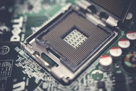
On a four-criterion comparison that drives most selections, the main ceramic options line up as follows [S2][S3][S4]:
1. Alumina (96–99.5%): thermal conductivity 20–30 W/m·K, dielectric strength >20 kV/mm, dielectric constant typically 9–10, lowest cost, suited to lower-power modules and general HV insulation.
2. Aluminum nitride (AlN): thermal conductivity 140–220 W/m·K, dielectric constant around 8–9, CTE close to silicon (≈4.5 ppm/K), higher cost, the default for IGBT/SiC modules and high-brightness LED carriers.
3. Silicon nitride (Si3N4): thermal conductivity 60–90 W/m·K, fracture toughness significantly above alumina and AlN, used where mechanical shock and thermal-cycling dominate (automotive power modules, traction).
4. DBC vs AMB on AlN: DBC is cheaper and proven on Al2O3, AMB is the reliable process for AlN and Si3N4, and AMB joints survive more thermal cycles before delamination in field data reported by substrate suppliers [S4].
Ceramics exhibit low dielectric constants, typically below 10, which reduces signal propagation delay and crosstalk on high-frequency circuits, making ceramic PCBs a credible alternative to FR-4 at gigahertz frequencies where organic substrates lose signal integrity [S3].
Semiconductor-Process and High-Purity Demands
Wafer-fab and semiconductor process equipment raise the bar: electrostatic chucks, plasma-resistant chambers, and vacuum feedthroughs require ±0.01 mm machining tolerance, cleanroom-compatible packaging, and contamination control that goes beyond what power-electronics substrates need [S2]. Dense alumina (99.5%+) and AlN are the standard material pair for electrostatic chucks because the combination of volume resistivity above 10^14 Ω·cm, high dielectric strength, and surface polish below 0.5 µm Ra supports the Johnson-Lambe and Coulomb-force chucking modes used in 300 mm wafer processing.
Ceramic substrate manufacturing uses metallization techniques matched to the application, with DBC (Direct Bonded Copper) and AMB (Active Metal Brazing) constructions applied to power module substrates that need combined electrical isolation and heat removal [S2][S3][S4]. Hermetic ceramic packages for optoelectronics, MEMS, and RF modules use metallized alumina or AlN lids with seam-sealed or solder-sealed Kovar frames, a construction that holds helium leak rates below 1×10^-8 atm·cc/s in qualified builds.
Selection Criteria and Common Sourcing Standards

Specifying ceramics for electronics starts with five concrete numbers: thermal conductivity target (W/m·K), dielectric strength (kV/mm), dielectric constant and loss tangent at the operating frequency, CTE match to the die or package, and the required surface roughness (Ra) for bonding or wire bonding. AlN is the right pick when thermal conductivity above 150 W/m·K and silicon-matched CTE are both required; dense alumina is the right pick when cost-per-part and dielectric strength dominate and thermal flux is moderate; Si3N4 is the right pick for automotive and traction modules where fracture toughness and thermal-cycling life are the constraint [S4].
Production quality is typically documented under ISO 9001:2015, with full dimensional inspection reports shipped per lot, and on-time shipment rates in the 95–100% band at established electronic-ceramic suppliers [S2].
For low-cost consumer electronics below about 10 W of dissipation, FR-4 or modified epoxy substrates deliver acceptable thermal performance at a fraction of ceramic cost, and the brittleness of ceramics adds yield risk in large-area panel processing. Alumina at 20–30 W/m·K is also a poor fit for high-current SiC modules above roughly 50 A per switch, where the thermal spreading bottleneck pushes junction temperature past the derating curve; AlN or Si3N4 is required in that range. [S3]
The supply picture is mature: alumina, zirconia, and titania remain the workhorse materials across electronics, medical implants, and industrial equipment, with electronic applications holding a consistent share of advanced-ceramics volume [S5][S6]. Ceramitec, the Munich trade fair, has scheduled its next electronics-focused edition for April 25–27, 2028, signaling continued OEM and tier-one supplier engagement with the segment [S1].
Engineers weighing substrate options should pin two trackable signals in the next sourcing cycle: whether the module's CTE and thermal-cycling profile put it in the AlN/Si3N4 band rather than the alumina band, and whether the required dielectric strength and insulation class push the insulator toward high-purity alumina or AlN rather than a polymer-mica stack. The wider context of industrial ceramic selection and industrial coating choices for harsh-environment electronics, plus the industrial adhesive systems used to bond ceramic to metal in DBC/AMB stacks, rounds out the spec map an engineer should keep in front of the BOM.