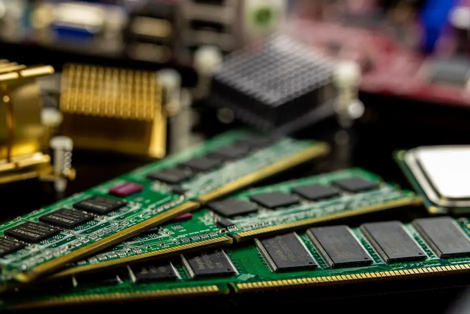
Per-chip memory bandwidth across the global AI accelerator fleet has compounded at approximately 4.1x per year through Q4 2025, with total shipped HBM bandwidth crossing 70 million terabytes per second [S4].
The driver is no longer training throughput. Modern LLM decode is memory-bandwidth bound: token generation streams every active weight from HBM to the compute units once per token, so the ceiling on tokens/sec equals memory bandwidth divided by active model size in bytes [S3]. Every generation therefore needs roughly 4x the per-chip bandwidth of its predecessor just to keep single-user latency flat as model weights expand.
The 4.1x-per-year compounding curve
Epoch AI's cumulative shipment tracker puts global AI-chip memory bandwidth at roughly 70 million TB/s by Q4 2025, with a year-on-year multiplier close to 4.1x sustained across the H100, H200, B100/B200, MI300X, MI355X, Trillium and Ironwood waves [S4]. In 2025, AI chips consumed over 90% of the HBM industry's revenue output, making the bandwidth curve effectively the demand curve for stacked DRAM itself [S4].
For a single accelerator, the per-device ladder spans roughly 1,300x, from 17 GB/s on a Raspberry Pi 4-class LPDDR4X channel at 4267 MT/s up to about 22 TB/s on a Vera Rubin-class datacenter GPU [S3]. That spread is what defines which model sizes can run interactively on which silicon.
Why decode, not prefill, sets the spec
LLM inference has two phases with opposite hardware profiles. Prefill processes the full prompt in parallel through dense matrix-matrix multiplications and stays compute bound, the regime classic FP8 tensor-core benchmarks measure [S3]. Decode, by contrast, reduces to matrix-vector multiplication: one skinny activation vector times a giant weight matrix per token, with compute units idle most of the cycle waiting on HBM [S3].
The arithmetic-intensity gap is what makes the bandwidth number the binding constraint. Because decode streams every active parameter once per token, the theoretical ceiling is simply bandwidth (bytes/s) divided by active model size (bytes), since the token generation phase of LLM inference is memory-bandwidth bound rather than compute bound [S3].
How much bandwidth each generation actually needs
The decode rule converts the model-size roadmap directly into a bandwidth roadmap. A 70B-parameter model at 4-bit quantization occupies roughly 35 GB of active weights, so a single user streaming at 30 tokens/sec needs at least 35 GB x 30 = 1,050 GB/s of HBM bandwidth just to feed the matrix loads, before any KV-cache traffic [S1][S3]. The commonly cited "greater than 1,000 GB/s" threshold for modern AI accelerators is exactly this floor, not a marketing number [S1].
Multi-tenant and long-context workloads push the requirement well past 1,000 GB/s per device. New Market Pitch documents a single 100,000-token Llama 3.1 70B session consuming about 30.5 GiB of uncompressed KV cache, with ten concurrent sessions reaching roughly 305 GiB before weights are counted, and one NVIDIA agent workload showing about 891,000 cached reads against 76,000 writes per session [S2]. Once context windows and agent loops dominate, per-GPU HBM bandwidth in the 3-5 TB/s class becomes the working minimum, which is the design point AMD's MI355X and NVIDIA's Rubin family target at 288 GB per device [S2].
Per-device comparison on the bandwidth ladder
Anchoring the ladder with sourced numbers makes the generational jump concrete. A consumer LPDDR4X channel at 4267 MT/s delivers about 17 GB/s, enough for a 1-2B model but capped near 17 tokens/sec on a 1 GB footprint [S3]. Datacenter accelerators in the H100 generation sit in the 3-4 TB/s per-device range, while the Rubin generation, alongside AMD's MI355X and Google's Ironwood TPU, moves per-chip bandwidth into the 8-13 TB/s band, paired with 288 GB of HBM per device [S2][S3].
On a like-for-like decode metric, the per-device bandwidth step from H100 to Rubin is roughly 3-4x, slightly below the 4.1x global compounded rate, with the rest of the growth coming from larger pod sizes: NVIDIA's Rubin NVL72 pools about 20.7 TB of combined HBM across 72 accelerators, and Google's Ironwood scales to pods of 9,216 TPUs [S2]. Aggregate pod bandwidth is therefore compounding faster than per-chip bandwidth, which is why interconnect (NVLink, ICI, optical) has become as much of a gating factor as HBM stack height.
Where memory is growing faster than GPU count
The 4.1x-per-year bandwidth number is not matched by a 4.1x-per-year increase in accelerator count per fixed workload. New Market Pitch frames this as a divergence: a 70B model at roughly 140 GB of weights fits on one AMD MI300X (192 GB) but not on one NVIDIA H100 (80 GB), so per-deployment hardware drops, while total fleet count keeps rising because served usage and model count keep rising in parallel [S2]. The economics test is shifting from "GPUs per model" to "cost per useful token delivered within a latency budget" [S2].
Software is closing part of the gap without new silicon. vLLM's original research reported roughly 2-4x throughput gains over earlier serving stacks, and Microsoft's OasisKV added up to 2.1x more throughput in specific long-context configurations, gains that come from KV-cache placement and paging rather than raw HBM bandwidth [S2]. The implication for spec writers: each hardware generation buys only part of the latency budget; the rest has to come from cache tiering, compression, and offload to cheaper memory.
Limits and failure modes of the bandwidth-first design
Bandwidth-bound decode has three predictable failure modes that the 4.1x curve does not solve on its own. First, KV-cache growth: long-context and agent workloads scale cache size with sequence length and session count, not with model size, so cache traffic can exceed weight traffic and force HBM redesigns around larger capacity rather than higher Gb/s/pin [S2]. Second, interconnect contention: at pod scale, all-to-all bandwidth across 72 to 9,216 devices becomes the binding constraint, and the same per-chip HBM number is wasted if the fabric cannot keep every device fed [S2]. Third, workload mix: prefill still scales with FP8/FP4 tensor throughput, so a chip tuned purely for decode can leave prefill underutilized on short prompts.
Operators are responding on the system side, not just the chip side: moving inactive KV into cheaper DRAM or NVMe, splitting prefill and decode across heterogeneous accelerators, compressing cached context, and re-routing requests to keep utilization high [S2]. Each of these trades memory-bandwidth headroom for software complexity, and each pushes the requirement that the next chip generation must at minimum match the 4.1x bandwidth curve to hold latency constant.
Trackable signals for the next cycle: HBM4 ramp timing and per-stack capacity (currently the binding lever above 288 GB per device), NVLink and optical-fabric roadmaps that determine whether pod bandwidth can outpace per-chip bandwidth, and the next published vLLM- or OasisKV-class serving stack that pushes cache efficiency past the current 2-2.1x software ceiling [S2][S4]. For a longer view of how this silicon is being deployed at the industrial edge, see edge AI silicon shifting to sub-5 nm NPUs and ASICs.