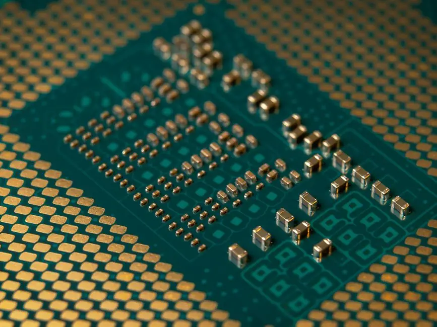
The semiconductor packaging market is projected to grow from $39.55 billion in 2025 to $43.01 billion in 2026, an 8.7% year-on-year increase, before accelerating to a 9.0% CAGR through 2030 to reach $60.64 billion [S1].
The growth engine is AI: TSMC stated on 2026-05-13 that the global semiconductor market is expected to exceed $1.5 trillion by 2030, up from its previous $1 trillion-plus target, citing AI-driven demand [S2]. Semiconductor packaging capacity, not raw wafer starts, is the binding constraint in 2026.
Market sizing: $39.55B (2025) to $60.64B (2030) at 9.0% CAGR
The Business Research Company's 2026-2030 forecast places the semiconductor packaging market at $43.01B in 2026 and $60.64B in 2030, a 9.0% CAGR for the 2026-2030 window, slightly above the 8.7% rate posted in 2025-2026 [S1]. That $17.6B of incremental revenue over five years is concentrated in advanced packaging, not legacy leadframe and QFN work.
Five named growth pillars underpin the forecast: AI-enabled semiconductor devices, 5G and wireless connectivity chips, automotive electrification, IoT deployment, and high-performance computing and memory [S1]. The first and last items map directly to CoWoS, SoIC, and HBM stacking; the others push fan-out wafer-level packaging (FOWLP) and embedded-die volumes for RF and power management.
Adjacent market context: the flexible packaging market is sized at $336.87B in 2025 and forecast to reach $432.74B by 2031 at a 4.26% CAGR, a much larger but slower-growing envelope that signals where food, pharma, and consumer-grade packaging demand sits relative to semiconductor-grade packaging [S4].
Technology mix: fan-out, 3D, and thermal materials lead the curve
Named technology trends inside the 2026-2030 forecast include fan-out and 3D packaging, enhanced integration of thermal management materials, growth in testing and quality assurance services, and a stronger focus on miniaturization and dense packaging [S1]. Fan-out and 3D are the structural shifts; thermal materials and test are the supporting infrastructure that scales with them.
Flip-chip and advanced packaging adoption are listed as part of the historic growth drivers that delivered the 8.7% 2025-2026 print, alongside consumer electronics, semiconductor manufacturing expansion, miniaturized device designs, and automotive electronics [S1]. For a spec engineer, this means the 2026-2030 ramp is not a step change in flip-chip; it is an extension of an already-deployed base into higher-tier nodes.
For background on who controls this capacity, see the 2026 vendor map by region and technology and the upstream wafer fab equipment market sizing, vendor map, and technology battle for the lithography and deposition side that feeds those packaging lines.
Application split: consumer electronics as volume base, AI as margin base
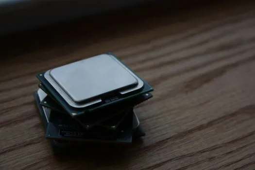
Consumer electronics, specifically smartphone and connected-device uptake, is the named primary driver of the 8.7% 2025-2026 growth [S1]. That volume base is what fills mature-node packaging lines, but it is the AI, HPC, and 5G cohorts that consume the 2.5D and 3D advanced-packaging capacity added in 2026-2030.
End-use sectors named as critical to the packaging step include consumer electronics, computing, telecommunications, automotive technologies, medical devices, and industrial electronics, with packaged devices playing roles in processing power, memory storage, sensing, and power management [S1]. Automotive electrification is singled out as a forward driver, with implications for power-module packaging at IGBT and SiC die sizes rather than at mobile SoC dimensions.
For the AI silicon layer above packaging, the wafer fab equipment 2026 vendor map covers ASML, Applied Materials, Lam Research, and Tokyo Electron, the suppliers whose EUV, deposition, and etch tools feed the CoWoS interposer and SoIC flows below.
Comparison of main packaging formats against 2026-2030 selection criteria
The mainstream options lined up against four selection criteria for 2026-2030 builds:
Flip-chip BGA: mature, broad OSAT supply base, lowest unit cost per pin, limited 2.5D scaling headroom; suited to networking ASICs and consumer SoCs. Fan-out wafer-level packaging (FOWLP): thinner profile, better electrical performance at mid pin counts, higher wafer-area utilization; the volume choice for RF and mobile PMICs through 2026-2030. 2.5D CoWoS / interposer-based: highest bandwidth for AI accelerators and HBM stacking, the binding-capacity node in 2026 with TSMC allocating the majority of the 2026 CoWoS output to AI silicon per the $1.5T 2030 framing [S2]. 3D SoIC / hybrid bonding: highest density and lowest pitch, the format with the steepest 2026-2030 capacity-add curve, but the most sensitive to thermal-management material integration listed as a 2026-2030 trend [S1].
Selection rule of thumb: if the die-to-die bandwidth requirement exceeds what an organic interposer delivers, or if HBM stacking is on the bill of materials, the build lands in CoWoS or SoIC; if not, FOWLP and flip-chip absorb the volume.
Standards, sourcing, and what a 2026-2030 spec sheet must lock down

Packaging specs in 2026-2030 are dominated by JEDEC register and dimension standards for BGA, WLCSP, and HBM stack geometry, IPC-9701 for thermal-mechanical performance, and IEC 60749 / JESD22 for reliability stress tests; these are the documents an OEM quality team will reference in a 2026 RFP, not a single market-forecast document. Equipment-side, the lithography and bonding tools that feed advanced packaging are covered by SEMI E84, SEMI E87, and the GEM300 communication standards, all of which the equipment vendor map above must integrate with. [S1]
Supply-side risk in 2026 sits in three places: CoWoS interposer capacity at TSMC, hybrid-bonding tool throughput at the OSAT tier, and thermal-interface material supply for 3D stacks, all of which the 2026 vendor map by region and technology tracks at the supplier level. For buyers building 2027-2030 roadmaps, the 9.0% CAGR [S1] should be read as a lower bound on advanced-packaging revenue and an upper bound on lead times for 2.5D and 3D capacity.
Track the next two signal nodes: TSMC's CoWoS monthly wafer-equivalent output update, typically revised quarterly, and OSAT capex disclosures from ASE, Amkor, and JCET for 2026-2027 fan-out and hybrid-bonding line additions; either a sustained CoWoS supply normalization or a Q3-Q4 2026 OSAT capex uplift will be the first hard evidence that the 9.0% CAGR is tracking.
For component-level specifications, see logistics packaging, packaging machine, and packaging material.