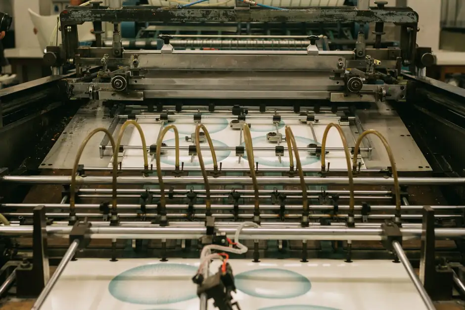
ASML captured 23.0% of the global wafer fab equipment (WFE) market in 2025, up from 15.5% in 2015, with a peak of 24.2% in 2023, a structural widening that has reshaped the four-vendor WFE core [S9]. SEMI's July 14, 2026 mid-year forecast puts 2026 WFE sales at $143.9 billion, a 23.1% year-on-year jump, with the segment projected to reach the $200 billion mark by 2028 [S1].
Applied Materials, Lam Research, and Tokyo Electron anchor the rest of the leading cohort, with KLA, ASM International, SCREEN Holdings, Hitachi High-Tech, Canon, Nikon, Advantest, Teradyne, Veeco, AIXTRON, EV Group, Kokusai Electric, ULVAC, DISCO, Plasma-Therm, and Oxford Instruments rounding out the public WFE vendor list cataloged by SNS Insider in March 2026 [S3]. The Lithography Equipment 2026: DUV Hold, High-NA EUV Push, and a Four-Vendor Core mapping covers the EUV/High-NA supply side that drives ASML's widening share.
WFE market sizing: 2025 baseline and 2026 to 2028 trajectory
SEMI's OEM-perspective forecast dated July 14, 2026 reports $116.9 billion in 2025 WFE sales, rising 23.1% to $143.9 billion in 2026, then 21.8% growth in 2027 and 14.1% in 2028 toward the $200 billion mark [S1]. Independent estimates diverge by methodology: SNS Insider values the broader WFE TAM at USD 36.85 billion in 2025 reaching USD 66.49 billion by 2035 at a 6.24% CAGR [S2], while Yole Group reports $129 billion in 2025 with a 9% CAGR to 2031 [S6], and Grand View Research values the wider semiconductor manufacturing equipment market at USD 118.88 billion in 2025 rising to USD 224.93 billion by 2033 [S5].
The dispersion reflects different scope boundaries: SEMI counts wafer processing, mask/reticle, and fab facilities equipment, while Yole and Grand View include back-end test and packaging. Market Data Forecast's 2026 estimate of $111.84 billion in 2025 growing to $268.06 billion by 2034 sits at the higher end of the range, illustrating how back-end inclusion shifts the headline number [S8]. The wafer-fab-only figure that process engineers spec against is the SEMI/WFE-defining number around $116.9 billion in 2025 and $143.9 billion in 2026 [S1].
Application mix: foundry leads at 40.1%, DRAM up 39% in 2026
Foundry and logic applications are projected to reach $78.0 billion in 2026, a 18.9% year-on-year increase, with the segment forecast at $104.7 billion by 2028 as 2nm gate-all-around high-volume manufacturing ramps [S1]. SNS Insider's March 19, 2026 breakdown places the foundry end-user at 40.10% WFE share in 2025, with the integrated device manufacturer (IDM) segment the fastest-growing at a 6.52% CAGR [S3].
Memory WFE is the steepest 2026 curve: DRAM equipment sales rise 39.0% to $38.8 billion in 2026, followed by 27.4% in 2027 and 15.0% in 2028 to reach $56.9 billion, while NAND equipment grows 30.7% to $13.9 billion in 2026 and 31.1% in 2027 [S1]. High bandwidth memory (HBM) is the named driver behind the DRAM acceleration, alongside advanced DRAM node migration and NAND technology transitions.
Vendor share: ASML at 23.0%, four-vendor core holds the rest
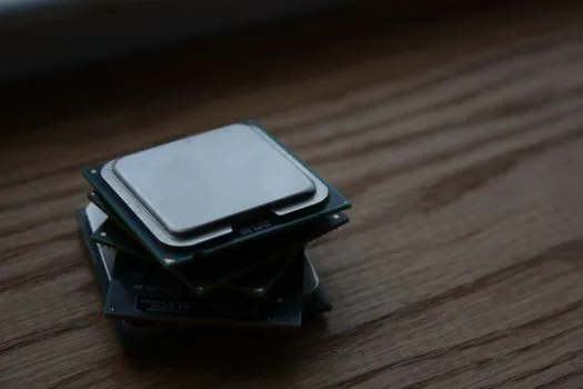
ASML's WFE share climb from 15.5% in 2015 to 23.0% in 2025 is the single largest structural shift in the vendor map, driven by the company's effective monopoly in EUV and emerging High-NA EUV scanner shipments [S9]. Applied Materials remains the largest non-lithography WFE vendor with broad deposition, etch, and inspection coverage; Lam Research holds the leading position in dielectric and conductor etch plus atomic layer deposition; Tokyo Electron dominates coater/developer tracks and certain deposition steps adjacent to EUV.
SNS Insider's vendor roster for the WFE market published March 19, 2026 lists 20 suppliers spanning lithography, deposition, etch, inspection, metrology, test, and assembly: ASML, Applied Materials, Lam Research, Tokyo Electron, KLA, ASM International, SCREEN Holdings, Nikon, Hitachi High-Tech, Advantest, Teradyne, Canon, Veeco, AIXTRON, EV Group, Kokusai Electric, ULVAC, DISCO, Plasma-Therm, and Oxford Instruments [S3]. KLA's standing in inspection and metrology, and ASM International's atomic layer deposition (ALD) leadership, are the most-cited specialty positions in the cohort.
Regional split: Asia Pacific 63.7%, North America 19%
Fortune Business Insights reports Asia Pacific dominated the semiconductor capital equipment market with a 63.7% share in 2025, reflecting Taiwan, South Korea, China, and Japan fab concentration [S7]. Business Research Insights values North America at 19% of the WFE market, with the United States contributing over 81% of regional demand, driven by data center and AI chip buildouts [S4].
SNS Insider's U.S.-specific WFE figure is $8.44 billion in 2025, projected at a 5.48% CAGR to $14.64 billion by 2035, with AI chips, data centers, and automotive electronics named as demand vectors [S2]. STMicroelectronics' March 2026 initiative to deploy more than 100 humanoid robots in legacy European fabs is a named automation play that the SNS Insider report flags as a productivity lever for older nodes [S2].
Technology and capacity mix: ALD at 35.5%, 300 mm at 51%
Automatic Layer Deposition held 35.50% of the WFE technology mix in 2025 and is the fastest-growing segment at a 7.38% CAGR through 2035, driven by thin-film deposition precision at advanced nodes [S3]. Etching, chemical vapor deposition, oxidation, and other processes make up the balance of the technology segmentation, with the SNS Insider report tracking five node-size brackets: below 5nm, 5-6nm, 6-14nm, 14-28nm, and above 28nm [S3].
The 300 mm wafer size segment commands 51.00% of WFE capacity in 2025, the dominant wafer format for advanced logic and memory, with 200 mm and 150 mm serving legacy and specialty nodes [S3]. Equipment for below 5nm process nodes is the named growth pole, with the broader transition to sub-7nm geometries identified as a structural WFE driver [S2].
Selection criteria: which WFE vendor fits which fab process
A fab process engineer choosing WFE suppliers typically ranks vendors on four axes: node capability (sub-5nm vs mature), technology segment (lithography, deposition, etch, inspection, test), regional service coverage, and tool throughput at the target wafer size. The four-vendor core of ASML (lithography), Applied Materials (deposition/etch/inspection breadth), Lam Research (etch/ALD), and Tokyo Electron (coater/developer/deposition) covers the critical process steps for leading-edge logic, with KLA, ASM International, and SCREEN Holdings handling inspection, ALD, and wet-clean specialty positions. [S3]
For sub-5nm and gate-all-around logic, ASML's EUV and emerging High-NA EUV systems are the only commercial path, making ASML a sole-source specification for those layers [S9]. For HBM-driven DRAM, Lam Research and Applied Materials etch and deposition tools dominate, while Tokyo Electron's coater/developer integration with EUV exposure is the de facto choice for advanced patterning. For mature nodes and 200 mm capacity, the long tail of Kokusai Electric, Hitachi High-Tech, ULVAC, and DISCO remains competitive on cost-per-wafer. Back-end test and assembly is led by Advantest and Teradyne, with the wider semiconductor test equipment segment projected at $15.3 billion in 2026, up 31.0% year-on-year [S1].
Limitations and sourcing caveats
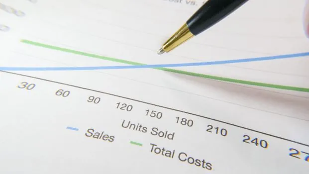
WFE market sizing diverges sharply between sources because scope boundaries differ: SEMI's $116.9 billion 2025 figure counts wafer processing plus mask/reticle plus fab facilities, while SNS Insider's $36.85 billion figure uses a narrower WFE-only definition, and Yole's $129 billion figure incorporates adjacent equipment categories [S1][S2][S6]. Vendor share percentages beyond ASML's documented 23.0% in 2025 are not consistently broken out in the public sources, making precise Applied Materials, Lam Research, and Tokyo Electron 2025 share comparisons qualitative rather than numeric.
Geopolitical and export-control developments are a structural risk to the WFE vendor map, particularly for shipments to China-based fabs, though the SNS Insider report cites this as a market-access constraint rather than providing shipment-level data [S3]. The wafer fab equipment (WFE) supplier base of 20 named vendors in the SNS Insider list is the most comprehensive public roster available as of August 2026 [S3]. SEMI's next full-year WFE forecast revision, typically released at the December SEMICON Japan, will be the next decision-grade data point; for application-level tracking, the quarterly TSMC and SK Hynix capex disclosures are the highest-signal public references for foundry and memory WFE demand.
Component reference pages worth checking: ndt equipment, anti static equipment, and construction machinery and equipment.