
Global chip packaging revenue reached USD 76.86 billion in 2025 and is projected to reach USD 144.18 billion by 2033, growing at a 7.6% CAGR, with Asia-Pacific controlling approximately 58% of the 2025 market [S2].
Advanced packaging, the higher-margin subset of the field, was valued at USD 51.65 billion in 2025 and is expected to grow to USD 140.38 billion by 2034 at an 11.75% CAGR, with flip-chip technology alone holding 48.2% of advanced packaging share in 2024 [S4]. A parallel estimate sizes the 2.5D and 3D packaging segment at USD 12.73 billion in 2026, growing to USD 24.18 billion by 2031 at 13.69% CAGR [S7].
Regional Share, 2025: Asia-Pacific Dominates, North America Recovers
Asia-Pacific accounted for roughly 58% of global semiconductor packaging revenue in 2025, anchored by OSAT (Outsourced Semiconductor Assembly and Test) clusters in Taiwan, China, South Korea, and Malaysia, with Taiwan's CoWoS expansion tied directly to AI accelerator and GPU supply chains [S2].
North America held around 25% of 2025 share, with growth tied to CHIPS and Science Act funding pushing the region from design-heavy dominance into advanced packaging and heterogeneous integration, even as high-volume back-end still depends on Asia-based OSATs [S2]. Europe held approximately 15% in 2025, strong in automotive-grade and power electronics, with EU Chips Act initiatives scaling localized capacity that still trails Asian leaders on advanced packaging throughput [S2]. The material side of the same ecosystem is a USD 19.11 billion market in 2025, projected to USD 38.51 billion by 2035 at 7.26% CAGR, with organic substrates and ceramic packages leading the product mix [S3].
Within the upstream toolchain covered in this Lithography Equipment 2026: DUV Hold, High-NA EUV Push, and a Four-Vendor Core read, advanced packaging's gains are downstream of front-end lithography choices, and EUV/HNA-EUAD decisions are now made jointly with 2.5D/3D back-end roadmaps at the major foundries.
Technology Mix: Flip-Chip Leads, 2.5D/3D and Chiplets Accelerate
Flip-chip packaging held 48.2% of advanced packaging market share in 2024, cited for superior electrical performance and high I/O density required by AI accelerators, GPUs, and high-end mobile processors [S4]. The 2.5D/3D IC packaging segment is forecast to grow from USD 12.73 billion in 2026 to USD 24.18 billion by 2031 at 13.69% CAGR, the highest growth rate in the stack, driven by HBM integration, silicon interposers, and chiplet architectures for AI workloads [S7].
3D IC and 2.5D IC packaging combined were valued at USD 66.96 billion in 2025 in one assessment, with a projection to USD 182.76 billion by 2035 [S8]. By material type, organic substrates contributed more than 42% of packaging material share in 2024, with bonding wires, lead frames, ceramic packages, and die-attach materials making up the balance [S1]. Over 70% of modern high-performance chips employ some form of advanced packaging per IC Insights data cited in 2026 market research, a penetration level that effectively makes "advanced" the new default at the high end [S4].
For comparison across the three main technology paths, flip-chip is the volume leader for high-I/O mainstream silicon, 2.5D/3D is the growth leader for AI and HBM-driven designs, and traditional lead-frame/BGA packaging remains the cost-optimized choice for analog, power, and mature-node devices, with the trade-off between cost, I/O density, and thermal performance driving the selection per die type.
Vendor Map: OSAT, Foundry Packaging, and IDM Capture
Custom Market Insights lists Amkor Technology (U.S.), ASE Group (Taiwan), ChipMOS Technologies (Taiwan), and Powertech Technology (Taiwan) as major packaging vendors in its competitive landscape, with Taiwan- and U.S.-headquartered players anchoring the publicly tracked OSAT tier [S5]. Within China, JCET and Tongfu Microelectronics are scaling fan-out wafer-level packaging (FOWLP), chiplet integration, and HBM packaging capacity to serve AI and mobile demand and reduce external supply-chain dependence [S2].
Foundry-affiliated packaging is increasingly competing with traditional OSATs as TSMC's CoWoS and similar in-house flows absorb high-end 2.5D/3D work, a structural shift that is reshaping the OSAT revenue mix toward advanced packaging and chiplet assembly rather than legacy test and assembly [S2]. The packaging materials ecosystem, dominated by substrate, bonding wire, and thermal management suppliers, is also consolidating, with Niching Industrial Corp. reporting NT USD 200 million in January-February 2026 revenue from AI-driven thermal products used in packaging and testing, a signal that thermal interface demand is tracking AI silicon volume [S3].
End-Use Mix: Consumer Electronics Leads, AI and Automotive Accelerate
Consumer electronics was the largest end-use segment in 2024, driven by smartphone and PC unit growth of approximately 4% globally, with Nvidia's overall semiconductor revenue up 56.4% in 2023 reflecting the AI accelerator pull-through that is reshaping packaging mix toward high-end 2.5D/3D [S1]. Gartner data cited in 2026 research shows data center processor shipments grew 12% in 2023, and Ericsson reports global 5G subscriptions surpassed 1.1 billion in 2023, both feeding the demand for advanced packaging throughput [S4].
Automotive semiconductor revenue is forecast to reach USD 200 billion on an annual basis by the mid-2030s, with EVs and ADAS pushing power-electronics and high-reliability packaging demand that favors ceramic and organic substrate packages over standard lead-frame designs [S1]. Smartphone production exceeded 1.4 billion units in 2023 per Yole Développement, sustaining flip-chip and FOWLP volume for mobile SoCs, RF, and power-management ICs [S4].
Constraints: Cost, Materials, and Thermal Bottlenecks
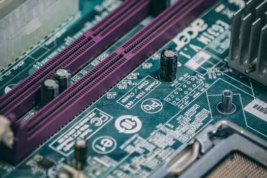
Advanced packaging processes require specialized equipment, cleanroom facilities, and precise alignment techniques, which raise unit costs and limit adoption among mid-sized electronics manufacturers, especially in cost-sensitive consumer segments [S4].
Specialized substrates, underfill materials, and solder interconnects face periodic supply shortages that can throttle high-volume throughput, with sourcing of thermally and electrically robust yet cost-effective materials remaining a persistent challenge in emerging supply chains [S4]. In 2026, 3DIC, Cu-Cu bonding, EMIB, and CoWoS technologies are all pulling on the same substrate and bonding-wire supply base that already supports the legacy packaging mix, and capacity additions in substrates and bonding wire are the rate-limiter on the 11.75% CAGR forecast for advanced packaging through 2034 [S3][S4].
Selection Map: Matching Packaging to Application
For AI accelerators and GPUs requiring HBM stacks and high I/O, 2.5D/3D packaging with silicon interposers is the only viable path, and lead times are gated by CoWoS-class capacity at Taiwan-based providers and at TSMC's in-house flow [S2][S7]. For high-volume mobile SoCs and consumer APs, flip-chip BGA and FOWLP deliver the best cost-per-I/O and the smallest footprint, with flip-chip's 48.2% advanced packaging share reflecting this volume dominance [S4].
For automotive and industrial power ICs, ceramic and high-reliability organic substrate packages remain the default, with EU-based vendors capturing share in this 15% European revenue slice and global automotive semiconductor revenue on track to USD 200 billion annually by the mid-2030s [S1][S2]. For analog, mature-node, and cost-driven ICs, traditional QFP, DIP, and standard lead-frame packaging still serves the bulk of unit volume and is the segment most exposed to OSAT competition from Chinese players scaling FOWLP and chiplet lines [S2][S5].
The key procurement signal for the next two quarters is substrate and bonding-wire supply, since 3DIC, EMIB, and CoWoS capacity additions are paced by upstream material availability rather than by packaging tool delivery [S3]. A second trackable signal is whether mainland China's FOWLP and HBM packaging lines at JCET and Tongfu move from mobile-grade volume to qualified AI-accelerator supply, which would shift regional share inside the Asia-Pacific 58% block [S2].
For component-level specifications, see logistics packaging, packaging machine, and packaging material.