
Glass core substrates moved from lab validation to pilot-line qualification in 2026, driven by AI and HPC interconnect density that organic BT and ABF laminates can no longer support at panel scale [S2][S9].
Intel confirmed in mid-2025 that its glass substrate program remains active, with launch readiness framed for the 2026-2030 window; the same program claims 10x greater interconnect density and 50% less pattern distortion than organic alternatives, alongside RDL features below 2 micrometers [S4][S5]. AGC, Corning, SCHOTT, HOYA, and Plan Optik together held 72.8% of the 2025 glass substrate advanced packaging market, with AGC alone above 21.5% [S5].
Material drivers: why glass beats organic and silicon interposers at the package core
Borosilicate and quartz glass offer a CTE that can be tailored across 3 to 10 ppm/degrees C, a dielectric constant of roughly 2.8 versus 12 for silicon, and an order-of-magnitude lower loss tangent than silicon at 40 GHz, which together deliver transmission losses suitable for sub-THz signaling [S3][S4]. At Ka-band and above, glass microstrip insertion loss is approximately half that of an equivalent organic line, and ultra-thin glass below 100 micrometers is already available in 700x700 mm sheets from LCD-derived panel processing [S3][S4].
Glass carriers 50% less warpage and 35% better positional accuracy than organic core substrates, which makes sub-2 micrometer redistribution-layer routing repeatable on large panels [S4]. For heterogeneous integration, research vehicles have demonstrated 60 chips mounted on a single glass substrate, a density level that organic laminates and first-generation silicon interposers cannot match without severe yield penalties [S1][S3]. The same TGV process that feeds RF redistribution can form vertical optical vias for co-packaged optics, so one glass core can carry both electrical and photonic layers [S3].
Adoption timeline: from R&D to pilot, and the 2026-2030 production window
2026 is the first year the technology crosses from R&D into pilot and qualification, with Samsung exploring glass cores alongside its I-Cube and H-Cube packages and SKC installing a pilot drill-and-fill line for 500 mm glass panels [S3][S9]. Intel has demonstrated glass-based test vehicles on its Arizona pathfinding line, AGC is shipping low-CTE borosilicate sheets for early evaluations, and no supplier has yet committed to a hard production launch date [S3].
Intel's roadmap frames launch readiness as a second-half-of-decade event, meaning 2026-2030 is the realistic envelope for first-volume shipments rather than a single calendar date [S2][S9]. ECTC 2025 papers already showed stacked glass architectures targeting greater than 100 GHz data rates, 6 micrometer TGVs at aspect ratios above 15, and predictive yield modeling for faster fan-out panel-level package ramps [S4].
Where glass fits, and where it does not
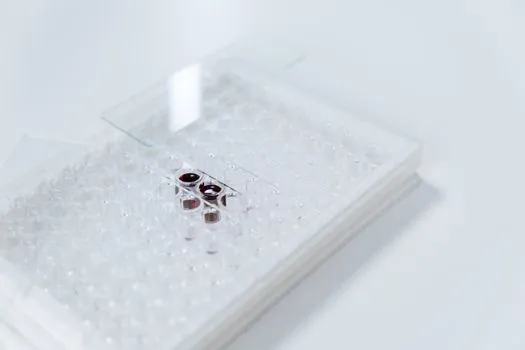
Glass is a credible answer for the largest, most routing-intensive compute packages where AI accelerators, high-bandwidth memory stacks, and optical engines must coexist on a flat, thermally matched surface [S5]. It is a poor fit for cost-sensitive consumer packages where BT and ABF organics still win on per-unit cost, and for ultra-fine-pitch chiplet wiring where silicon interposers remain the only proven route until glass TGV yield matures [S3][S4].
Glass dicing still risks microcracking, repeatably fabricating thousands of fine-pitch TGVs at panel scale remains unsolved, and a hybrid glass-organic or glass-ceramic core layer is the most realistic transitional architecture rather than a clean material swap [S2][S4]. A senior engineer spec'ing a package today should treat glass as a qualification-track option for AI and HPC sockets, not as a drop-in laminate replacement across the full product portfolio [S5].
Selection criteria for a glass-core build
Match glass CTE to the die at 3-7 ppm/degrees C for silicon-side attachment, and to the PCB at the upper end of the 3-10 ppm/degrees C window for board-level reliability [S1][S4]. Use a panel size that leverages LCD supply chain economics: 500 mm and 700x700 mm formats are already in pilot, and the per-unit cost of glass is expected to converge toward high-end organics as panel yield improves [S3][S4]. Specify TGV pitch and aspect ratio explicitly, since 6 micrometer vias at aspect ratios above 15 are state of the art and 2 micrometer RDL is the design floor that glass enables today [S4].
Plan for the metrology gap: suppliers that can deliver stable via metallization, low-defect panel processing, and credible reliability data will secure design-ins before vendors offering glass composition alone, because qualification evidence carries as much weight as nominal substrate performance [S5]. Buyers who want a low-risk entry should engage with the advanced material supply chain through existing packaging material channels, since the same borosilicate ecosystem that feeds MEMS capping and wafer-level fan-out carriers is the upstream feed for packaging-grade glass cores [S3].
Standards, sourcing, and the manufacturing bottleneck
Glass is already a quiet incumbent inside the fab: ultra-flat borosilicate carriers hold wafers during backside thinning, sodium-free sheets form hermetic MEMS caps, and low-CTE glass is the baseplate for many wafer-level fan-out processes, so the supply base and inspection toolchain exist even though the packaging application is new [S3]. The UCIe chiplet standard accelerates the demand side, because heterogeneous integration of compute, memory, and I/O tiles is the workload that justifies routing density only glass and silicon can deliver [S7].
The practical competitive boundary is the TGV and panel-handling learning curve, not the glass composition, and that favors integrated suppliers with co-development capacity over standalone glass vendors [S5]. For a complete read on how this material shift ties into broader semiconductor materials cycles, see the germanium supply-gap analysis, which tracks a parallel critical-materials squeeze affecting photonic and RF packaging roadmaps.
Trackable signals through 2027
Watch for Intel's first disclosed production-grade glass substrate package ship date inside its 2026-2030 envelope, and for SKC's 500 mm panel pilot output crossing internal qualification milestones in 2027 [S3][S9]. Track Samsung's I-Cube and H-Cube roadmap updates for any glass-core variant, and watch for AGC, Corning, and SCHOTT capacity announcements at 510x515 mm or 700x700 mm panel formats, since panel size is the lever that closes the cost gap to high-end organics [S3][S4][S5].
For component-level specifications, see logistics packaging.