
HBM3e stacks 8-high or 12-high DRAM dies with a 1024-bit interface across 16 independent channels, delivering over 1.2 TB/s per stack, and HBM4 doubles the per-stack bandwidth target to 2.0 TB/s by widening the interface to 2048 bits when production begins in 2026 [S1].
Three memory makers (SK hynix, Samsung, Micron) currently supply HBM3e volume, and the equipment toolset for HBM centers on through-silicon via (TSV) etch, TSV copper-fill deposition, atomic layer deposition (ALD), wafer thinning, micro-bump or hybrid bonding, and known-good-die test, rather than on front-end logic lithography [S1][S2].
HBM architecture defines what the equipment must do
HBM is a 2.5D/3D-stacked DRAM packaged with a logic die on a silicon interposer, connected by thousands of fine-pitch traces (about 2,048 data lines plus roughly 1,000 command, address, and clock traces between one HBM stack and the host processor) [S5].
Vertical connections use TSVs, microscopic copper-filled holes etched through each thinned DRAM die, which is why HBM is described as a high-rise of chips with TSVs acting as elevators between floors [S5][S2]. HBM3e increases per-pin data rates from 9.2 to 12.4 Gbps, and HBM4 pushes that further while adding all-around power TSVs to cut IR drop by up to 75% versus HBM3 [S1].
Stack heights have grown from 8-high (24 GB) to 12-high (36 GB) at HBM3e, with HBM4 expected to scale further; each die in the stack is thinned to roughly 30-50 micrometers before bonding, which sets hard limits on wafer-handling robotics and chuck flatness in the bonding tool [S1][S2].
Core equipment set: TSV etch, copper fill, ALD, bonding
For HBM3 and HBM3e, the tool chain is dominated by deep silicon etch (Bosch-process or cryogenic DRIE) to define TSV holes, followed by barrier and seed deposition, copper electrochemical deposition (ECD) to fill high-aspect-ratio vias, and anneal [S2].
Lam Research explicitly markets the Syndion etch system for TSV hole definition, the SABRE 3D deposition family for TSV copper fill and interconnect layers, and ALD tools for the precise oxide and barrier liners required as aspect ratios climb in higher-stack HBM generations [S2].
Wafer thinning to single-digit tens of micrometers, temporary carrier bonding/debonding, and die-stacking with thermo-compression or hybrid bonding are the next gate, and hybrid bonding is required for sub-10-micrometer pitch interconnects that future HBM4E-class stacks will need [S5][S2]. Metrology in-line (CD-SEM, IR interferometry for TSV depth, acoustic microscopy for void detection) and known-good-die burn-in at the stack level round out the line [S4].
Selection criteria when the buyer is an OSAT or memory maker
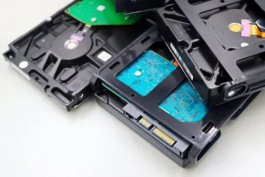
For TSV etch, the binding specs are silicon etch rate, sidewall taper (typically targeted under 89-90 degrees for void-free copper fill), selectivity to the hard mask, and TSV aspect ratio capability, with HBM3e stacks needing aspect ratios in the 10:1 to 20:1 range depending on via depth [S4][S2].
For copper-fill deposition, the binding specs are bottom-up fill rate, post-fill CMP dishing control, and resistance uniformity across-wafer, because TSV IR drop is one of the dominant HBM3e power-delivery limiters that HBM4 power-TSV redesigns are trying to relieve [S1][S2].
For bonding tools, the binding specs are placement accuracy (sub-1-micrometer for hybrid bonding at 3-micrometer pitch and below), bond-force uniformity across a 300 mm wafer, and thermal budget control so that DRAM cell retention is not degraded by high-temperature steps; for ALD, the spec is sub-1% thickness uniformity on high-aspect-ratio TSV sidewalls [S2][S4].
Comparing main tool categories on four decision criteria
Buyers evaluating HBM-specific back-end tools typically line up TSV etch, TSV/copper ECD, wafer-level bonding, and ALD against four criteria: throughput (wph on 300 mm), achievable aspect ratio or pitch, COO per wafer, and readiness for 12-high or taller stacks [S4][S2].
TSV deep silicon etch scores high on throughput (Lam-class tools run tens of wafers per hour in production) and on aspect ratio (10:1 to 20:1 verified for HBM3e), but COO per wafer is elevated by mask, gas, and chamber-clean chemistry costs; for HBM4 taller stacks, etch vendors must extend aspect ratio without sacrificing sidewall taper [S2].
TSV copper ECD tools are competitive on aspect ratio (void-free fill at 10:1 and beyond) and on COO (copper chemistry is relatively cheap), but throughput is constrained by long fill times on high-aspect-ratio vias and by metrology that must catch voids at the via bottom, where the highest current density and the highest IR drop concentrate [S1][S2].
Wafer-level bonding tools (thermo-compression for HBM3e, hybrid bonding for HBM4 and beyond) sit at the top on alignment accuracy (sub-1-micrometer, with hybrid bonding pushing toward sub-0.5-micrometer) but are the throughput bottleneck of the line, because each die-stack requires per-die placement and anneal, and tool uptime is sensitive to particle control [S2][S5]. ALD is the lowest-throughput step but is non-negotiable as a barrier/liner step, and oxide thickness uniformity below 1% across the TSV sidewall is the spec that determines whether downstream copper fill stays void-free [S2].
Who this equipment is for, and who it is not for
TSV etch, copper ECD, and hybrid-bonding tools in the HBM class are designed for 300 mm wafer fabs running stacked-DRAM volume, and for OSATs building advanced-packaging lines that partner with memory makers on 2.5D integration, not for legacy back-end assembly lines that only do wire-bond or flip-chip at pitches above 40 micrometers [S4][S5].
Buyers that only need flip-chip bumping at 100-micrometer pitch, or wire-bond packaging for analog and power ICs, do not need the HBM-class tool set: the throughput, alignment, and metrology overheads of TSV and hybrid bonding cannot be justified for non-stacked-dRAM products, where a standard linear guide on a wire bonder or flip-chip tool is the right spec [S4].
Conversely, a fab that plans to move into HBM4 hybrid bonding within 24 months should not buy an HBM3e-only thermo-compression bonder, because sub-3-micrometer pitch requires hybrid bonding with embedded metal pads, and a tool that cannot be field-upgraded to that process will become stranded capital [S2][S5].
Limitations, failure modes, and yield risks
The most common yield killer in HBM TSV processing is incomplete copper fill, which leaves a void at the via bottom and shows up as a high-resistance TSV or an open die in stack-level test; void detection by IR interferometry or acoustic microscopy is therefore a hard process-control gate, not an option [S2][S4].
Wafer thinning beyond about 30 micrometers makes the stack mechanically fragile, so handling robotics and temporary-carrier adhesive selection are recurring line-down risks, and die warpage at the 12-high level forces bonding tools to compensate with sub-micrometer Z-height control per die [S1][S2].
Hybrid bonding has its own failure mode: misalignment beyond about 0.5 micrometer at the die-to-die interface causes immediate yield loss, and surface contamination (particles below 100 nm) blocks copper-copper bonding and creates opens that only show up at known-good-die test [S5]. For non-stacked lines using anti-static equipment and standard pick-and-place, these failure modes do not apply, but the spec discipline does carry over: cleanroom class, ESD control, and metrology resolution follow the same physics.
Standards, sourcing, and signals to track
There is no single HBM-specific industry standard; the relevant documents are JEDEC HBM3 and HBM4 specifications, which define the per-pin data rate, channel count, and physical interface, while equipment-side standards are inherited from front-end fab practice (SEMI E10 for yield management, SEMI E84 for carrier handling, and SEMI standards for 300 mm FOUP/EFEM interoperability) [S1][S4].
For procurement, lead times on hybrid-bonding tools and high-aspect-ratio ECD systems ran 12-18 months through 2025 as HBM demand grew from 123 million GB in 2022 to a projected 972 million GB by 2027, and tool vendors publicly named in the HBM-specific space include Lam Research (Syndion, SABRE 3D, ALD) [S2]. The three memory makers currently shipping HBM3e volume are SK hynix, Samsung, and Micron [S1].
Two trackable signals to watch into 2027: first, whether the HBM4 2048-bit wide I/O actually ships in 2026 as planned, because that determines whether hybrid bonding moves from R&D to high-volume manufacturing; second, whether TSV aspect-ratio and bonding alignment specs tighten in published JEDEC updates, since each step drives a new tool generation [S1][S5].
For the relevant spec sheets and selection criteria, see additive manufacturing material.
For related coverage, see Ferrosilicon Demand Outlook 2026-2030: Steel, EAF and Solar Drive the Spec.