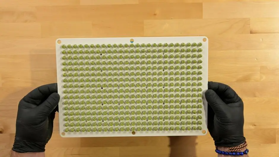
Common microbolometer array formats today include 320×256 and 640×512 pixels, with pixel pitch migrating from 17 µm to 12 µm and now toward 10 µm and 8 µm across commercial thermal imaging cameras [S2][S4][S7].
Pixel pitch is the centre-to-centre spacing between adjacent detector elements on the focal plane, while pixel size refers to the physical dimensions of the same element, the two terms are used interchangeably in vendor literature [S3][S9].
Pixel pitch, pixel size, and array area: the geometry behind the number
Sensor width equals horizontal pixel count multiplied by pixel pitch, and reducing pixel pitch should allow a proportional reduction in the focal plane array size [S5].
For a fixed horizontal pixel count, smaller pitch narrows FOV unless the lens is redesigned, because FOV is governed by sensor width and focal length through FOV = 2 × arctan[(sensor width / 2) / focal length] [S1].
The instantaneous field of view (IFOV) equals pixel pitch divided by focal length, so 12 µm pixels paired with the same focal length as 17 µm pixels deliver 1.42× finer angular sampling, a directly measurable spatial-resolution gain that does not require changing the optical housing [S1].
Field examples in vendor material show that with 90 µm-class pitch (legacy pyroelectric arrays) the illuminated footprint covers roughly 13.9 pixels of the target image, illustrating how pitch sets the absolute spatial sampling limit before any processing [S6].
17 µm vs 12 µm vs 10 µm: a side-by-side decision comparison
On the same 8-inch wafer, a 12 µm pitch design for a 384×288 array yields several times the die count of a 25 µm pitch design, with 17 µm delivering over 200 dies, and 12 µm delivering over 300 dies per wafer, directly lowering per-sensor cost as pitch drops [S3].
For a fixed FOV, smaller pitch allows a shorter effective focal length, enabling shorter, lighter, cheaper germanium or chalcogenide lens assemblies and supporting the trend toward compact handheld and OEM modules [S1][S3][S5].
Thermal sensitivity (NETD) and spatial resolution are independent: NETD is governed by pixel area, fill factor, and readout noise, while spatial resolution is governed by pitch and optics, so a 10 µm sensor can be thermally inferior to a 12 µm sensor even though it is spatially finer [S1][S4].
Pitch, NETD, optics fit, and cost form a 4-criteria comparison: 17 µm pairs the highest per-pixel SNR and most relaxed lens MTF with the largest focal plane; 12 µm hits the practical sweet spot used in current mainstream 640×512 modules; 10 µm and 8 µm shrink the optical envelope and raise pixel density but demand faster optics and advanced readout compensation to keep NETD within usable limits [S1][S2][S3][S8].
Why pitch is shrinking: wafer yield, optics, and recognition distance

Pixel size in commercial detectors has trended from 45/30/25 µm down through 17/15/12 µm to current 10 µm and 8 µm designs, with 8 µm now identified as the next-generation target for higher pixel density [S3][S8].
Smaller pitch enables longer recognition distance at the same focal-plane footprint: more pixels across the same die allow finer angular sampling, so a target of given size can be identified at greater range when optics support the sampling rate [S3].
From a 2025 SPIE analysis, reducing pixel pitch allows a proportional reduction in both focal-plane-array size and effective focal length, the core scaling relationship that has driven the move from 17 µm to 12 µm and now to 10 µm in OEM modules [S5].
Per Raytron field experience, 6 µm and 8 µm modules can underperform 12 µm modules in image clarity because the smaller fill factor reduces per-pixel photon collection, lowering SNR and raising temporal noise unless compensated by advanced readouts, microlens arrays, or pixel binning [S1].
Application-driven pitch selection: short range, long range, OEM
For short-range, detail-critical use cases such as PCB inspection, handheld diagnostics, and OEM integrated assemblies, smaller pitch (8 µm or 10 µm) is technically attractive but only pays off when the lens MTF and image-processing pipeline are matched to the new sampling rate [S1][S7].
For mid-range industrial and security thermal cameras, 12 µm pitch in 640×512 or 1024×768 formats remains the dominant production choice, balancing yield, NETD, and optical compatibility with off-the-shelf lenses [S3][S4][S7].
For long-range observation and surveillance modules, 17 µm pitch in larger arrays is still common because per-pixel SNR and the resulting NETD advantage extend identification range under low-contrast atmospheric conditions, even though pixel count per square millimetre is lower [S3][S4].
The thermal imaging camera and thermal imager categories both now span 10 µm, 12 µm, and 17 µm offerings from multiple OEMs, so buyers should match pitch to optical stack rather than defaulting to the smallest number on the datasheet [S2][S7].
When smaller pitch backfires: NETD, fill factor, and lens MTF
A small pixel alone does not guarantee a clearer image: if the lens MTF is limited at the sensor's Nyquist frequency, the extra pixels capture noise rather than additional detail, and the system behaves as if the pitch were still larger [S1].
Reduced fill factor at 8 µm and 6 µm shrinks the active detector area per pixel, cutting infrared energy collected and degrading NETD unless microlens arrays concentrate incoming flux onto each element or binning merges adjacent pixels at the cost of resolution [S1][S8].
For OEM integration projects, the typical decision sequence is to lock FOV and detection range first, then size the lens, then select the smallest pitch that the chosen lens can resolve, which in practice often means a 12 µm sensor rather than a 10 µm or 8 µm sensor [S1][S7].
When higher pixel density is mandatory, designers can mitigate NETD loss by selecting sensors with lower-noise ROICs, by averaging neighbouring pixels in firmware, or by accepting a narrower operating-temperature range, since NETD drifts with detector temperature [S1][S4].
Standards, sourcing, and what to track next
No single IEC or ISO standard fixes pixel pitch values for thermal imagers; pitch is a manufacturer-disclosed performance parameter, while NETD, spectral response, and environmental testing are governed by the detector's datasheet and by application-specific standards such as IEC 60079 for hazardous-area thermography [S1][S4].
Tracking the migration: 8 µm pitch is now flagged by sensor manufacturers as the next mainstream target above today's 10 µm and 12 µm production lines, while 6 µm remains largely experimental in commercial microbolometer modules [S1][S8].
Two signals worth watching are the appearance of 1024×768 or larger focal-plane arrays at 10 µm pitch, which would mark the next cost/yield crossover, and OEM modules that bundle 8 µm sensors with matched high-MTF lenses as integrated units rather than as bare detectors [S1][S5][S7]. See also this process engineer's note on thermal camera NUC behaviour for the related calibration-side constraints that interact with pitch selection.