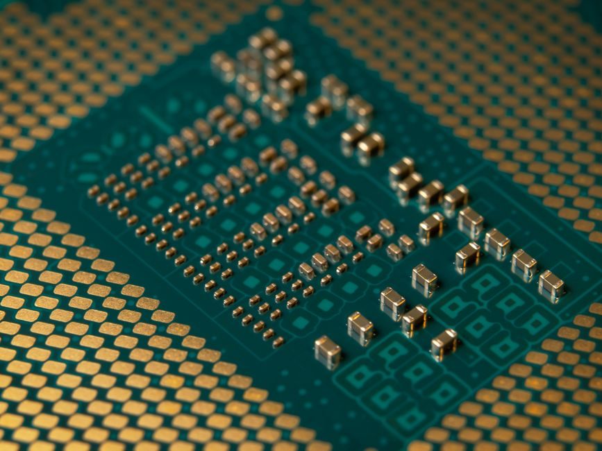
MEMS sensor unit cost is governed by four building blocks: front-end wafer fabrication, MEMS-specific process modules, wafer-level or die-level packaging, and final test, with wafer fab and packaging typically absorbing the largest share of the bill of materials [S1][S3].
Unlike a pure CMOS ASIC, every MEMS die carries mechanical or thermal structures, so the process flow adds deep-reactive-ion etching (DRIE), wafer bonding, LPCVD/PECVD polysilicon, and release steps on top of standard IC lithography and doping [S2][S3].
Wafer Fabrication: Mask Count, Node Choice, and Diameter
Mask count and wafer diameter set the floor of MEMS cost. MEMS flows often run 10-20 mask layers, with each additional mask adding lithography, etch, deposition, and inspection cost on top of the base CMOS process [S3].
Foundry services such as LioniX International process SOI (silicon-on-insulator) wafers and add DRIE, LPCVD, PECVD, wet etching, oxidation, sputtering, evaporation, and wafer bonding as billable modules, so a custom flow stacks 6-10 extra process steps beyond a baseline CMOS run [S2].
Substrate choice also matters: piezoresistive pressure sensors from NOVOSENSE are processed on silicon wafers through the company's own MEMS micro-machining line, with every wafer AOI-inspected on front and back side to comply with AEC-Q103 [S5].
MEMS-Specific Process Modules and Equipment Loading
DRIE is the single most expensive MEMS module. It drives deep silicon etches with alternating etch and passivation cycles, runs slower than standard plasma etch, and requires dedicated tools that are not always available on a generic CMOS line [S2][S3].
Wafer-level packaging (WLP) is the second major cost driver: capping wafers, glass frit or anodic bonding, and through-silicon vias (TSVs) for pressure and inertial parts add cap-wafer cost, bond alignment time, and yield loss on top of the device wafer [S2].
LPCVD polysilicon, used for structural layers and known for stress control problems, demands high-temperature operation and dedicated furnace time, while PECVD amorphous silicon is chosen as a low-temperature alternative below 110 °C when budget or substrate constraints rule out LPCVD [S3].
Packaging, Test, and Calibration Cost Levers

After wafer fab, the back-end absorbs a large share of the per-die cost. Semiconductor test houses listed in the 2026 Anysilicon catalog separate wafer sort, final test, and burn-in, so each step appears as a distinct line item on the test quote [S1].
For high-reliability parts, AEC-Q103 compliance adds wafer-level AOI on front and back side plus device-level qualification, increasing per-die test time before a MEMS pressure or inertial sensor can ship to automotive Tier-1s [S5].
Companies such as Integra Technologies package die preparation, assembly, test, and characterization as a turnkey Hi-Rel flow, while Custom Silicon Solutions lists "Sensors & MEMS Expertise" alongside mixed-signal ASIC design, confirming that sensor test programs are quoted separately from standard IC flows [S1].
Process Selection: How the Choices Move the Number
Node choice and process selection dominate the cost stack. Shifting from 65 nm to 40 nm CMOS ASIC base roughly trades mask count and wafer area against performance, and MEMS layers add on top of whatever node is chosen, not instead of it [S1].
For a displacement sensor or flow sensor that needs mechanical travel, designers must keep the mechanical layer and the CMOS ASIC on the same or bonded wafer, so packaging cost is set by the MEMS cap and not just the IC.
For parts that need electrical readout only, a capacitive sensor signal chain can use a smaller mechanical structure and standard IC packaging, trimming the per-die cost versus a fully hermetic pressure or inertial package.
Infrared thermopile and pyroelectric MEMS from MFrontier sit on a different cost curve because the MEMS die is hybridized with a separate readout ASIC, so assembly and test dominate while wafer fab cost per die is comparatively low [S6].
Foundry Engagement Models and What They Cost
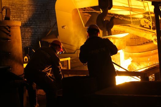
A pure foundry path, where the customer owns the mask set and the fab only runs wafers, minimizes fab NRE but leaves the customer paying for MPW shuttles, mask revisions, and yield ramps on every step [S2].
A turnkey ASIC model, as offered by Tekmos, Cyient Semiconductors, and Pacific MicroCHIP, folds design, fab, packaging, and test into a single quote, which lifts the per-part price but removes the customer's exposure to mask and yield surprises [S1].
Fabless specialists such as CSS keep design, sensors, and mixed-signal blocks in-house, then buy wafer, packaging, and test from merchant vendors, so the cost stack is transparent but requires the customer to manage multiple suppliers and qualifications [S1].
Total Cost of Ownership: NRE, Yield, and Lifetime
NRE is dominated by mask sets, bond-fixture design for wafer-level packaging, and the test program; on low-volume MEMS programs these one-time charges can equal several years of unit cost, so amortization volume is the first number a spec engineer should pin down. [S1]
Yield loss in MEMS comes from particle-induced stiction, residual stress in structural layers, and cap-wafer misalignment, all of which are quoted back into the unit price through foundry yield-loss assumptions, and long-term drift in the field adds warranty reserve on top of manufacturing cost [S3].
Operational cost drivers include power, which is why consumer IMUs such as the STMicroelectronics LSM6DSL family target 0.65 mA in high-performance mode with always-on features, and calibration cost, which is set by test time and trim hardware at final test [S7].
Standards, Certification, and Sourcing Discipline
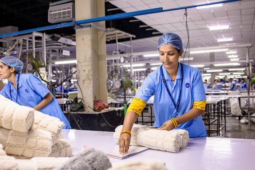
AEC-Q103 is the dominant MEMS-specific stress-test standard for automotive pressure and inertial sensors, and it is met at the wafer level through AOI plus device-level qualification on the NOVOSENSE NSP1832 platform [S5].
Process control methods taught in university programs, such as the CU Boulder "Sensor Manufacturing and Process Control" course, treat statistical process control on etch rate, thin-film stress, and bond alignment as the levers that protect MEMS yield across a production run [S8].
Sourcing discipline follows the same pattern: an inductive sensor or LVDT sensor spec that piggybacks on a MEMS process flow should be sourced from a vendor that can quote fab node, MEMS module count, package type, and test program separately, because the same mechanical performance at very different unit prices is usually a different mix of these four cost blocks.
Trackable signals for the next planning cycle: foundry MPW calendar updates from LioniX International, AEC-Q103 revision notes, and any new foundry-process modules released under additive manufacturing material flows that target MEMS packaging [S2][S5].
Related analysis: Pharmaceutical Equipment Market 2026: Three Sizing Tracks for Spec-Driven Buyers.