Quartz material installation is not one workflow but several, because the family spans fused silica, single-crystal quartz, and engineered stone, each with different thermal, optical, and mechanical acceptance windows [S1][S2].
For semiconductor lines, the dominant forms are fused quartz crucibles for silicon single-crystal growth, fused quartz bell jars for lithography, and single-crystal quartz blanks for SAW and piezo devices; each demands a different mounting strategy [S2].
Define the Quartz Grade Before You Specify the Mount
Fused quartz and fused silica carry service ratings up to roughly 1100 °C in continuous use, with softening points near 1650 °C and an extremely low thermal expansion coefficient near 0.55 × 10⁻⁶ /K, which is the property process engineers exploit when bell-jar or wafer-carrier distortion would scrap a batch [S2]. Fused quartz is normally specified in semiconductor and optical applications under names such as Corning 7980, OHARA SK1300, or Schott Borofloat 33, all of which the quartz material reference class lists as fused-silica substrates rather than true single-crystal material [S2]. Single-crystal quartz, by contrast, is anisotropic and is cut along specific crystallographic axes (X, Y, AT, SC, ST, BT) to set the resonance temperature and frequency behaviour; mis-orientation shows up as frequency drift, mode coupling, and reduced Q, not as visible damage [S2].
Pre-Install Inspection: Dimensional, Optical, and Surface Checks
Fused-quartz bell-jar and tube shipments should be unpacked in a cleanroom class 1000 (ISO 6) or better environment, then wiped with isopropyl alcohol (typically 99.9 % electronics grade) and inspected under collimated white light; surface scratches deeper than about 0.1 mm and inclusions larger than 0.3 mm are typical reject criteria, though the OEM drawing is always the binding document [S2]. For single-crystal quartz blanks, confirm the orientation marking (X-, Y-, Z-axis scribe or laser etch) and the flat orientation against the purchase order; AT-cut blanks are most common for 1 to 250 MHz fundamental-mode oscillators because the frequency-temperature curve flattens near 25 °C in that orientation [S2].
Thickness, flatness, and parallelism should be verified with a micrometer or optical interferometer at a minimum of five points (centre, four corners) before any mounting; standard semiconductor-grade blank flatness is typically λ/10 at 633 nm, and surface roughness below 1 nm Ra is common for optical-grade wafers [S2]. Wafer-grade fused silica substrates are generally supplied to thickness tolerance of ±0.025 mm for 100 mm and 150 mm diameters, with total thickness variation (TTV) below 10 µm, which is the binding acceptance gate for cassette-loading tools.
Mounting Methods by Component
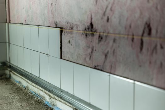
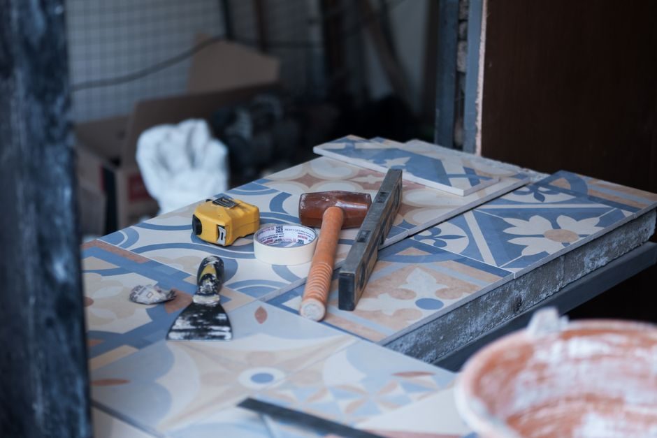
Bell jars and large fused-quartz tubes are typically clamped at the flange only; the wall section is left free so thermal expansion can run axially. The clamp load should be torque-controlled to the OEM value, and a compliant gasket — typically unfilled PTFE or Viton for low-temperature service, graphite for high-temperature diffusion — sits between the quartz flange and the metal flange. Engineered quartz slabs in countertop or work-surface service are dry-set on a level substrate with 3 mm shim stacks at 200 to 300 mm centres, then seam-joined with colour-matched acrylic adhesive and clamped for 15 to 30 minutes; seams are sanded at 220 then 400 grit, and full cure is 24 hours before loading [S4][S6].
Single-crystal quartz blanks are mounted inside hermetic packages using conductive silver-filled epoxy or silicone-based die-attach, with bond-line thickness held to 0.02 to 0.05 mm; cold welding or Au-Sn eutectic bonding is used for high-reliability military and aerospace devices. The mounting clamp design must apply uniform pressure, since the material is brittle and concentrated loads will chip the edge. Comparison gate for selecting the mount approach:
Quartz-grade vs mount-method matrix — (1) Fused quartz bell jar / tube: flange clamp only, no side load, PTFE or graphite gasket, thermal expansion free; (2) Single-crystal quartz blank for SAW/piezo: conductive epoxy or Au-Sn eutectic, 0.02 to 0.05 mm bond line, orientation-locked package; (3) Wafer-grade fused silica substrate: vacuum chuck or edge-grip cassette, 3-pt contact to avoid backside particle generation; (4) Engineered quartz slab: dry-set on shimmed substrate, seam-bonded, 24 h cure.
Thermal, Cleanliness, and Pressure Acceptance Tests
After mount, a leak-rate test on sealed fused-quartz assemblies typically targets a helium leak rate below 1 × 10⁻⁹ mbar·L/s for semiconductor process chambers. For high-purity diffusion and oxidation tubes, a high-temperature vacuum bake-out at 200 °C for 4 hours followed by a 1000 °C soak for 2 hours is a common burn-in to outgas residual moisture and binder; the rate of temperature rise should not exceed 5 °C/min to keep thermal-stress gradients low, because the material's low thermal conductivity (about 1.4 W/m·K for fused quartz) means a fast ramp can crack a thick wall [S2].
For piezoelectric quartz blanks, post-mount acceptance includes frequency verification on a network analyser or impedance meter against the target (for example 38.4 MHz ±10 ppm for industrial TCXO references), series resistance below about 25 Ω, and a motional-capacitance ratio consistent with the cut. The quartz material grade selected determines the test limits: an SC-cut is preferred for oven-controlled oscillator (OCXO) use because of its lower stress sensitivity, while AT-cut covers the wider fundamental-mode range [S2]. A sample spec sheet line — "AT-cut, 25.000 MHz, Ci 4.0 fF, Cp 5.0 pF, Rr ≤ 25 Ω, Q ≥ 30 000" — illustrates the kind of acceptance document to keep on file per lot.
Failure Modes, Limits, and When to Replace
Quartz components fail in three dominant ways, and each has a different repair-or-replace gate. (1) Thermal-shock fracture: visible cracks running from the wall, usually after a ramp above 10 °C/min or a cold wet load into a hot chamber; the only corrective action is full replacement, since cracked fused quartz loses vacuum integrity and sheds particles into the process. (2) Devitrification: a cloudy crystalline surface layer that forms on fused quartz above about 1000 °C in the presence of trace alkali or water vapour; this is progressive and signals end-of-life for high-purity diffusion work, even if the part is mechanically intact [S2]. (3) Contamination staining: metallic or organic films on optical surfaces, often removable with the right acid wash (for example, piranha solution at 80 °C for organic residues, or dilute HF for silica haze), but the etch rate is roughly 0.1 to 0.3 µm per minute in dilute HF, so the cleaning step itself must be measured to avoid thinning a precision surface beyond tolerance.
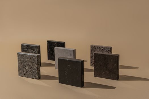
Engineered quartz slabs fail differently — chip at cutouts, seam yellowing, and impact cracks from dropped pans. Chips under 5 mm can be filled with colour-matched resin and re-polished; cracks longer than 25 mm or those running through the seam line call for slab replacement, since the polymer matrix has already cracked and the failure will propagate under thermal cycling [S4][S6].
Sourcing, Standards, and Records to Keep
For semiconductor and optical grades, request the lot's mill certificate listing OH content (typically below 200 ppm for Type I fused quartz, 800 to 1000 ppm for Type II), trace-metal analysis, and birefringence class; this is the data that supports a low-defect-count wafer-process claim [S2]. The quartz material family, including fused silica, kaolin, cordierite, steatite, and fireclay, falls under the broader silicate-material supplier set, and many US distributors concentrate the inventory regionally — Clarks Summit, Pennsylvania is one such node [S1].
For end-use traceability, keep a per-install record of grade, lot number, orientation, mount torque, leak-rate result, and thermal-cycle history. Related spec-driven process-engineering reads worth pairing with this guide: Sputtering Target Pros, Cons, and Selection Map for the next material decision in a deposition line, and Data Center Manufacturing Equipment Guide 2026: From Wafer Fab to White-Glove Decommission for the wider fab-to-decommissioning chain. One trackable signal to watch: an OEM publish date for a fused-quartz grade with sub-1 ppm alkali content, which is the next tightening the semiconductor industry is signalling.
Spec-level background on the components involved: linear guide, and crossed roller guide.