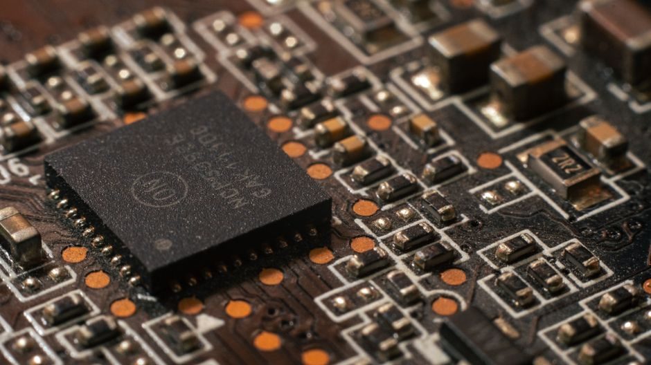
Semiconductor manufacturing equipment (SME) is the production tooling set spanning front-end wafer fabrication and back-end assembly/test, and the segment is on track to expand from USD 166.35 billion in 2025 to USD 344.36 billion by 2032 at an 11.0% CAGR per MarketsandMarkets [S5].
The expansion is being pulled by high-performance computing and AI training/inference data-center build-outs, which force advanced-node wafer-fab capex and back-end advanced-packaging capacity to scale in lockstep. Process-engineering buyers now select from a Japanese global-niche supplier base — Shibaura Mechatronics advertises coverage from front-end to back-end process equipment on its 2026-06-03 product page [S1] — and from European distribution channels such as SiSTEM Technology (UK, +44 (0)1327 362 844) that handle lab-to-fab R&D and production gear [S6].
SEMI E137: The Packaging, Shipping, and Relocation Reference
SEMI E137-0705 (Reapproved 1111)-2011, "Guide for Final Assembly, Packaging, Transportation, Unpacking, and Relocation of Semiconductor Manufacturing Equipment," is the 9-page international benchmark that defines how an SME, sub-assembly, or component leaves the supplier's dock and is accepted into a high-purity or ultra-high-purity cleanroom [S2].
The standard applies end-to-end — from final assembly and packaging at the supplier's facility, through shipment, all the way to uncrating and re-positioning inside the customer's cleanroom manufacturing area. Its Chinese mirror, GB/T 29845-2013, carries the same scope and citation graph, giving Chinese fabs a direct local reference for site-acceptance workflows [S3]. For any project engineer taking delivery of a multi-million-dollar tool, the E137 check-list is the first document to keep on the receiving dock.
SEMI E35: Cost-of-Ownership Metrics That Drive Buy Decisions
SEMI E35-0307-2006, "Guide to Calculate Cost of Ownership (COO) Metrics for Semiconductor Manufacturing Equipment," is the 22-page industry reference for building an apples-to-apples COO model across lithography, etch, deposition, inspection, and back-end tools [S4].
The guide covers any equipment that processes a semiconductor unit — wafers, devices, flat-panel displays, or other substrates — and notes that some terminology is specific to integrated-circuit wafer and device production. A practical takeaway for 2026 sourcing teams: COO inputs must include tool purchase price, footprint and facility hook-up (chilled water, exhaust, ultra-pure water, gas cabinets), consumable yield loss, MTBF/MTTR, and throughput in wafers-per-hour, then the E35 formulas normalize those into comparable cost-per-wafer metrics that procurement can negotiate against. This is the same cost-engineering logic that surfaces in related buy-side categories such as the Coding Machine TCO: 5- to 10-Year Cost Stack, Driver Map, and Sourcing Specs breakdown — capital equipment is capital equipment, and the same five-year stack applies.
Front-End vs Back-End Equipment: Criteria Comparison
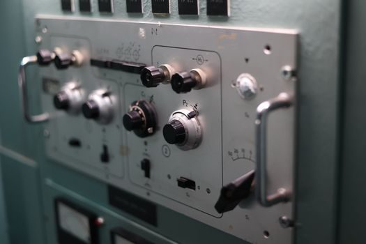
Front-end tools run on 300 mm (and emerging 450 mm R&D) wafer cassettes inside ISO Class 3 or cleaner cleanrooms, with sub-nm overlay and single-digit-nm defect control — examples include lithography, plasma etch, CVD/PVD deposition, CMP, ion implant, and metrology. Back-end tools handle dicing, die-bond, wire-bond, flip-chip, molding, and final test, often on strip-format or panel-format carriers in ISO Class 5-7 environments [S1].
On four decision criteria the two sides differ sharply: (1) cleanroom class — front-end ISO 3 / Class 1, back-end ISO 5-7 / Class 100-10,000; (2) throughput units — front-end wafers-per-hour, back-end units-per-hour or strips-per-hour; (3) primary COO driver — front-end tool price and yield loss dominate, back-end consumables and labor often outweigh tool price; (4) vibration/abatement sensitivity — front-end requires sub-µm vibration isolation and point-of-use abatement, back-end tolerates standard facility floors. For plants riding the AI-driven capex wave, advanced packaging back-end (HBM stacking, 2.5D / 3D integration) is closing the precision gap with front-end, which is why 2026 sourcing plans must treat both sides together rather than as separate capex buckets — a constraint also visible in the HBM Memory Shortage 2026: Structural Supply Squeeze, Wafer Allocation, and Sourcing Risk coverage.
Selection Criteria: Who SME Buys Are For, and Who Should Skip
Buyers of front-end SME are typically IDMs and foundries running 28 nm and below logic, DRAM, or 3D NAND, with 300 mm fabs costing USD 10-20B+ each, where COO analysis under SEMI E35 [S4] and E137-compliant receiving [S2] are non-negotiable.
Buyers of back-end and lab-scale SME include OSATs, advanced-packaging specialists, compound-semiconductor lines (SiC, GaN, GaAs), MEMS and photonics fabs, and university/industrial R&D centers — categories where SiSTEM Technology's lab-to-fab sales and service model [S6] is typical. Skip SME sourcing if you only need consumer-grade electronics assembly, PCBA, or general contract manufacturing — back-end SME is overkill, and a Industrial Barcode Scanner Buying Guide 2026-class automation tier will cover traceability instead. SME is also a poor fit where production runs are sub-100 units/year; the COO math under E35 will not amortize tool price, install, and facility work.
Market Size, Capex Drivers, and 2026 Signals
The market was valued at USD 166.35 billion in 2025 and is projected to reach USD 344.36 billion by 2032, implying an 11.0% CAGR through the forecast window, with high-performance computing and AI training/inference data-center expansion as the principal demand engines [S5].
Two trackable signals for 2026 are: (a) HBM and advanced-packaging capacity additions, where the squeeze documented in HBM Memory Shortage 2026 is already pulling back-end tool orders forward, and (b) the shift of COO scrutiny onto facility hook-up cost and ultra-pure water / ultra-pure gas / abatement budgets — the area where SEMI E35 [S4] gives buyers the cleanest negotiating lever against OEMs. Shibaura Mechatronics' own positioning — "global niche top products" covering both front-end and back-end [S1] — confirms that mid-cap Japanese and European suppliers are still setting the SME niche-product benchmark alongside the lithography and deposition majors. For fab planners mapping their next capex cycle against the USD 344.36B 2032 figure [S5], the Edge Computing Gateways Anchor Smart Manufacturing Data Plane layer above the tools — and the Industrial Ethernet for Smart Manufacturing backbone underneath — should be sized in the same budgeting pass, not bolted on after tool delivery.
For the relevant spec sheets and selection criteria, see additive manufacturing material, anti static equipment, and linear guide.