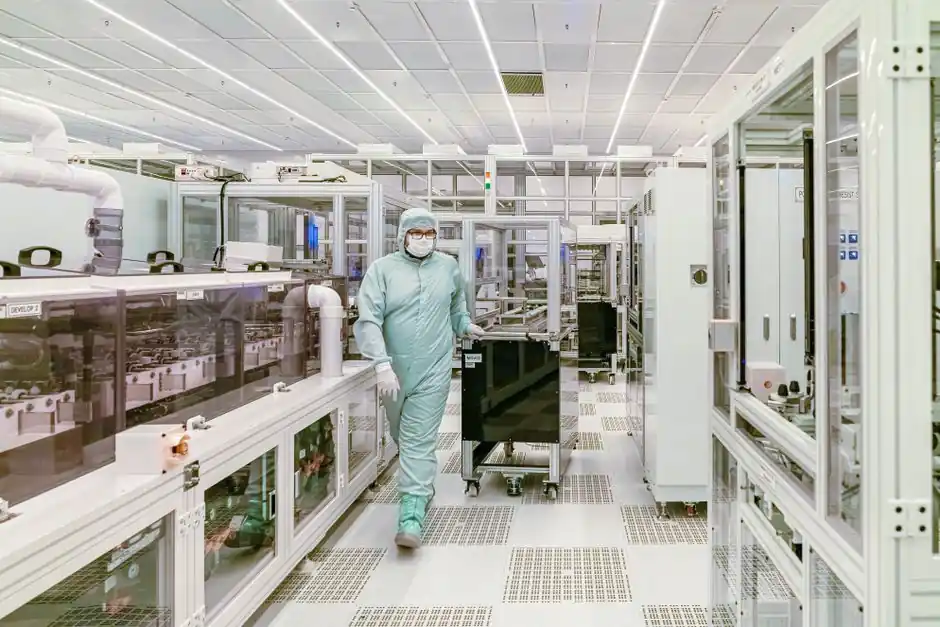
OLED panel fabs in 2026 rely on a tightly choreographed chain of vacuum deposition, encapsulation, and laser tools rather than a single machine, with vacuum thermal evaporation (VTE) remaining the dominant process for organic layer stack formation and linear evaporation sources sized for 4.5G, 6G, and the new 8.6G substrate generations [S1][S5].
Process Classification: Dry VTE vs Wet/Solution Routes
OLED deposition splits into dry and wet method families, with dry VTE converting solid organic powder into vapor that condenses onto a substrate in a solid-phase layer, the textbook baseline for the small-molecule OLED stack [S5].
Wet methods, including Seiko Epson's inkjet-printed OLED HDTV approach disclosed in 2009, target large-area cost reduction by avoiding the FMM shadow mask change cycle and the per-evaporation-source material waste, but adoption remains limited to specific RGB-sidewall and sol-gel encapsulation niches [S1].
Within dry VTE, the UHV cluster platform has become the default building block: Polyteknik A/S, for example, integrates thermal evaporation, RF/DC sputtering, E-beam evaporation, and Knudsen cells for organic deposition in one cluster, a configuration sold in multiple units to OLED research lines [S1].
Deposition Tool Map: VTE, MBE, E-beam, Knudsen, Sputter
For organic layers the workhorse is VTE with Knudsen-type effusion cells feeding linear sources, while metal cathodes and injection layers route through E-beam evaporation or RF/DC sputtering chambers in the same UHV cluster [S1].
Riber (Euronext: RIB) supplies molecular beam epitaxy (MBE) systems and dedicated diffusion cells and sources targeted at OLED display production, a different value proposition from R&D MBE: in-line uptime and source-packing density, not ultrahigh vacuum base pressure alone [S1].
For OLED R&D and pilot lines, Scienta Omicron's OFT EDGE Series can both deposit and analyse organic and inorganic layers on flexible or solid substrates in a single vacuum environment, which is why it appears so often in published OLED stack studies [S1].
Flexible OLED Tool Chain: ELA, LLO, Polyimide, Lamination
Flexible OLEDs on polyimide require an extra process module set that rigid glass fabs skip: ELA for crystallising the polyimide buffer, LLO for separating the finished panel from its carrier glass, and a lamination station for the final curved or flat cover [S1][S4].
Screen Holdings (formerly DaiNippon Screen Mfg) through SCREEN Finetech sells deposition machines for flexible OLED production on polyimide substrates and announced new 6-Gen OLED deposition systems in November 2017, while its Screen Laminatech subsidiary offers a flexible OLED lamination tool that bonds panels to curved glass, with R&D units shipping and mass-production tools planned [S1].
Schiller Automation (a Kurtz Ersa subsidiary) packages the cluster into factory automation, building complete production lines for photovoltaic, automotive, electronics, and OLED display and lighting customers, which is the level at which a new fab actually purchases equipment rather than individual chambers [S1].
Encapsulation, Gettering, and Source Materials
Encapsulation, not the organic stack itself, is usually the lifetime bottleneck on a flexible OLED line, and the SAES Group sells both electron-injection material sources for VTE and a portfolio of encapsulation materials and getters targeted at organic and flexible electronics [S1].
Sealed getters matter because OLED cathodes are reactive and edge ingress through TFE pinholes kills operational lifetime; SAES' high-purity vapor release and shape-memory alloys are specified into the same encapsulation cluster that runs the TFE CVD head [S1].
For the deposition side, the practical trade-off is between FMM VTE (mature, fine pixel pitch, slow mask change) and open-frame VTE (faster, coarser pitch, used in tandem white-OLED with colour filters), with most Gen-6 flexible phone lines in 2026 still running the FMM VTE variant for RGB [S1][S5].
Test, Repair, and Yield Equipment
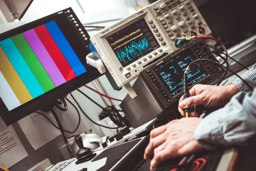
Seichi Technology (JIngzhida Technology), established 2011 in Shenzhen, supplies testing, calibration, and repair systems for the display and memory industries, with OLED-specific offerings in optical inspection, display aging, gamma adjustment, and mura compensation [S1].
Inline mura compensation, in particular, is a high-leverage tool class: one photometric mura-comp cell positioned after cell test can recover several percent of panels that would otherwise be reworked or scrapped, which on a 6-Gen line at roughly 30,000 substrates per month is a non-trivial throughput number [S1].
Laser-Based Tools: LLO, ELA, and Micromachining
Newport markets pulsed and ultrafast laser systems, high-fluence optics, and high-speed precision positioners specifically packaged for OLED panel processing, where excimer laser annealing (ELA) of the polyimide buffer and laser lift-off (LLO) of the carrier glass are the two critical thermal-budget steps [S4][S6].
Flat panel display manufacturing as a whole is moving from LCD to OLED and from glass to flexible plastic substrates, and laser patterning and cutting of the multilayer organic stack, rather than the glass itself, drives the choice of femtosecond or nanosecond pulse widths on these tools [S4].
The same source notes that heterogeneous multilayer organic stacks demand high-quality, high-accuracy laser processing, which is why a single laser platform is rarely sufficient: LLO, ELA, scribing, and repair each need different pulse widths, fluences, and beam-shaping optics [S4][S6].
Selection Criteria and Vendor Shortlist
For a new Gen-6 flexible OLED line the practical vendor map in 2026 is: Polyteknik or Riber for cluster VTE/MBE chambers, Screen Finetech for 6-Gen deposition and Screen Laminatech for cover lamination, SAES for getters and injection sources, Schiller Automation for the line-level integration, and Newport or MKS-supplied laser platforms for ELA/LLO [S1][S4][S6].
For research and pilot lines under, say, 200 mm x 200 mm substrates, the Scienta Omicron OFT EDGE deposition/analysis cluster and the Polyteknik UHV PECVD platform cover most needs, with Seichi supplying the optical and aging test cells downstream of the deposition tool [S1].
Buyers should also plan the procurement of additive manufacturing material reference coupons for chamber-fixture prototyping, because OLED cluster fixtures increasingly use metal-polymer hybrid jigs built with the same additive process families used in semiconductor capital equipment [S1].
Standards, Sourcing, and What to Watch Next
OLED equipment itself is not governed by a single IEC or ISO standard the way pressure vessels are; buyers instead reference SEMI standards for cluster-tool mechanical interfaces, fab-wide洁净度 classes, and hazardous-gas delivery, layered with regional safety codes for the vacuum and laser subsystems [S4][S6].
The decisive cost variables in 2026 are substrate generation (8.6G tools command a 1.5x to 2x multiplier over 6G for the same chamber count), encapsulation yield (a 1% TFE pinhole-density drop is worth more than a 5% organic-stack throughput gain), and the FMM mask changeover time on VTE, which is the single largest hidden production-rate penalty on rigid RGB lines [S1][S5].
Trackable signals for the next planning cycle: 8.6G deposition tool deliveries from Screen Finetech and AP Systems, the ramp of sol-gel and inkjet-printed OLED lines for monitor panels, and any move by Seiko Epson or a Chinese OEM to bring solution-process RGB back into the small-molecule Gen-6 tool set [S1]. For a parallel view of how 2026 display-panel retrofit decisions are being made across other capital equipment, see the Display Panel Industry 4.0 retrofit protocol map.
Spec-level background on the components involved: linear guide, and crossed roller guide.