
China-sourced NAND flash in 2026 splits cleanly into two lanes: small-density (512Mbit-4Gbit) SPI/parallel parts from Fudan Micro, GigaDevice, XTX, and Zetta for industrial designs, and high-density 3D NAND from YMTC for AI and data-center workloads [S1][S2][S4].
Industrial buyers specifying chips for -40°C to 85°C operation can source SLC-grade SD NAND, SPI NAND, and parallel NAND with hardware ECC, wear levelling, and power-loss protection through Shenzhen-based distributors, with single-piece MOQs available for prototyping and standard lead times of roughly 6 weeks on stocked part numbers [S3][S4].
Cell Type and Endurance Trade-Offs
SLC NAND remains the only cell type suitable for write-intensive industrial logging, with endurance rated at roughly 100,000 program/erase cycles versus 1,000-3,000 for MLC/TLC and 100-1,000 for QLC, per the indicative range published in the CNFX component reference [S1].
For most embedded control and IoT designs, the practical choice is SLC SD NAND or SLC SPI NAND at 512Mbit-4Gbit, where the 8-bit or 16-bit hardware ECC and block-management firmware are integrated into the package. Higher-density TLC and QLC parts only make sense when the host controller can handle the heavier wear-levelling and read-disturb mitigation, typically in SSD or eMMC form factors, not raw NAND [S1][S4].
Interface, Voltage, and Package Specs
The two interfaces that matter for industrial buyers are SPI (single/dual/quad) for low-pin-count designs and parallel (ONFI or Toggle Mode) for high-throughput storage. Fudan Micro's SPI NAND line covers 512Mbit to 4Gbit at 2.7V-3.6V, with the FM25S005B at 512Mbit in TDFN-8 and the FM25S01B/FM25S04B stepping up to 1Gbit and 4Gbit respectively [S2].
SD NAND parts from XTX (XinTianxia) ship in LGA and WSON packages with built-in hardware ECC, wear levelling, and power-loss protection, with industrial grades covering -40°C to 85°C; GigaDevice GD5F-series parts such as the GD5F1GQ5UEYIGR sit in the same slot at 1Gb SLC in WSON-8 [S3][S4]. For a quick spec on similar electronic-component sourcing discipline, see this pressure transmitter selection guide.
JEDEC Compliance and Test Discipline
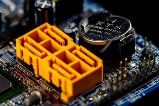
JEDEC JESD84 (eMMC) and JESD209 (UFS) are the governing standards for managed-NAND packages, while raw NAND follows JESD230 and the ONFI/Toggle Mode specifications. Reliability testing under JEDEC includes data-retention bake, temperature cycling, endurance cycling, and read-disturb characterisation, with voltage tolerance typically held at ±5% and timing parameters at ±10% on industrial-grade parts [S1].
Buyers should ask for the JEDEC test report, not just a marketing datasheet, and verify the part number against the legal manufacturer's PCN (process change notification) log. Distributors that ship with traceability documents and a signed specification sheet are the only ones worth running through qualification, even if their unit price is higher than spot-market resellers [S1][S3].
Supply Continuity and Lifecycle Risk
The largest supply risk in 2026 is not capacity, it is obsolescence on small-density SPI/SD NAND part numbers. AI-driven demand pulls 3D NAND fab capacity toward 128-layer and above TLC/QLC die, squeezing mature-node lines that produce 1Gbit-4Gbit SLC [S4][S7].
For a project that needs 3-7 years of supply, lock the part number with a written PCN undertaking, qualify a second source on the same footprint, and watch the 6-week standard lead time for small-density Chinese SD NAND as the early-warning signal. XTX, GigaDevice, and Fudan Micro all maintain standard part-number inventories; distributors quoting longer lead times on a previously in-stock part are signalling an allocation event, not a normal backlog [S4].
Comparison of Main Sourcing Options
For B2B buyers, the four most relevant Chinese NAND suppliers in 2026 are Fudan Micro (SPI NAND, EEPROM, automotive-grade temperature), GigaDevice (SPI NOR, SPI NAND, eMMC at scale), XTX (SLC SD NAND, LGA/WSON packages, focus on small-capacity embedded), and YMTC (3D TLC/QLC with Xtacking architecture for high-density and AI workloads) [S2][S4][S7].
On four decision criteria: cell-type coverage runs Fudan (SLC) < GigaDevice (SLC/TLC) < XTX (SLC SD NAND) < YMTC (3D TLC/QLC); industrial-grade temperature support is broadly available across Fudan, GigaDevice, and XTX but not on YMTC's consumer 3D lines; supply continuity on small-density parts is strongest at Fudan and GigaDevice, weakest at YMTC where AI demand competes for wafer starts; pricing on a per-bit basis is lowest at YMTC and highest on Fudan's automotive-qualified SPI NAND. The decision rule: specify Fudan or GigaDevice for 512Mbit-4Gbit industrial designs, XTX for SD-NAND-form-factor drop-in replacements, and YMTC only when the design needs 64Gb or more with managed controller [S2][S4][S7]. A parallel cross-walk of this gate-style selection method appears in Sourcing DRAM from China: 2026 Spec Map and Supplier Gate.
Procurement Gate Checklist for RFQ Release
Four checks must close before a purchase order is released: (1) JEDEC-compliant datasheet with revision history; (2) confirmation of operating temperature grade (commercial 0-70°C, industrial -40-85°C, automotive -40-105°C); (3) ECC scheme matched to the host controller (typically 8-bit per 512 bytes for SLC, 16-bit or stronger for TLC/QLC); and (4) supplier transparency on legal entity, factory address, and warranty terms [S1].
Unit price on Alibaba- and Accio-style B2B platforms ranged from roughly $0.01 for low-density 16Mbit SPI NOR/NAND to $10-24 for 128-256Gbit eMMC managed-NAND packages in August 2026, with single-piece MOQs offered by Shenzhen distributors for prototyping and volume tiers kicking in at 100-1,000 pieces [S3]. Treat any quote below $0.10 on a 1Gb SLC part as a counterfeit or remark risk until lot-trace documents are provided, and run incoming inspection per AOI and lot traceability style documentation discipline. The wider pattern of four-gate spec mapping for industrial electronic components is detailed in DRAM Procurement 2026: A Four-Gate Spec Map for B2B Buyers.
Watch Items for the Next Two Quarters
Track three signals through Q4 2026: YMTC's Xtacking Gen 3 rollout and whether 128-layer/232-layer TLC pricing crosses below $0.05/GB on 1Tb die; the JEDEC UFS 5.0 standard ratification, which will set the managed-NAND roadmap for 2027 mobile and edge-AI designs; and the 6-week small-density lead-time baseline at XTX and Fudan, which historically inverts to 12+ weeks within 4-6 weeks of an allocation event [S4][S7].
Spec-level background on the components involved: linear guide.