
Industrial and embedded buyers in 2026 face a NAND market where 3D stacking past 200 layers, QLC/PLC adoption, and PCIe 5.0 transition reshape per-gigabyte cost while shifting the qualification burden onto firmware and ECC [S3].
The procurement decision is no longer "which chip is cheapest" but a three-axis trade between cell endurance, interface bandwidth, and supplier commercial stability, with spot prices for commodity SPI NAND in the $0.08–$5.30 range and 1Gb SLC TSOP parts hovering around $0.50–$2.99 [S2][S5].
Cell-type endurance bands and the SLC-to-QLC decision
SLC remains the reference floor for write-heavy industrial workloads, with SLC/MLC P/E cycle ratings above 100,000 cycles, versus TLC and QLC which trade endurance for density in consumer and read-mostly designs [S8]. Pseudo-SLC (pSLC) mode, which operates TLC NAND as if it were SLC, gives designers a cost-down path when true SLC is over-spec'd but bare TLC endurance is unacceptable [S4].
For datasheet claims, modern industrial controllers use LDPC ECC capable of correcting hundreds of bit errors per page, and the headline UBER (uncorrectable bit error rate) figure, often around 1e-15, is only as good as the wear-levelling and read-disturb management around it [S4]. QLC and PLC raise the density ceiling but demand sophisticated controllers; planners should treat endurance budget as a firmware problem as much as a silicon problem [S3].
Interface tiers: ONFI, PCIe, eMMC, and SPI NAND
Raw NAND interface selection drives both throughput and qualification scope. ONFI 3.2, 4.1, and 5.0 are the major raw-NAND compliance points buyers must match to their host controller, with 1.2 V core voltage, 8 KB page size, and 1,200 MT/s speeds typical at the 176-layer node [S2][S6]. For embedded designs, eMMC 5.1 parts such as the KLM4G1FETE-B041 deliver 300 MB/s read / 19 MB/s write at 4 GB capacity in a 153-ball BGA, while managed NAND like the SDIN7DU2 family at 16–128 Gb integrates the controller internally [S2][S5].
For designers wiring SPI rather than parallel, Winbond's W25N01GVZEIG at 1 Gb in WSON-8 and the W25N02KVZEIR with Dual/Quad SPI buffer read are common pick-list parts, and GigaDevice's GD5F1GQ5UE/GD5F2GQ5UE series covers the 1–4 Gb SPI NAND window at $1.42–$5.30 spot [S2][S5]. On the high-performance end, NVMe/PCIe Gen4 and Gen5 client and edge SSDs are taking share for AI and data-centre workloads, with suppliers like Micron shipping a 9th-generation (G9) 3D QLC NAND at 2 Tb die and 3.6 GB/s, a direct read of where per-die density is heading for the next 12–18 months [S9]. Buyers should map their interface to the host ASIC's IP, not the marketing brochure, because Gen4 controllers cannot negotiate Gen5 speeds, and Gen5 hosts add BOM cost that consumer products often cannot recover.
Industrial vs. consumer flash: six procurement gates
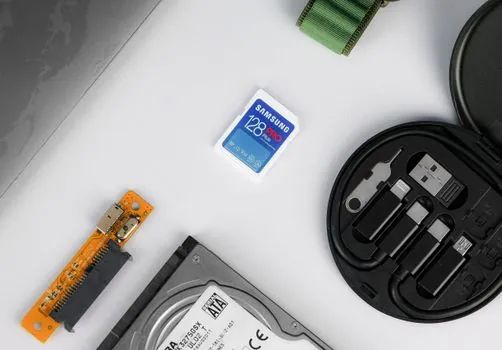
Industrial-grade flash is differentiated on six dimensions, and ticking only one or two is not enough for a 10-year product [S4]. Operating temperature range must be −40 °C to 85 °C, versus 0 °C to 70 °C for consumer parts. Endurance is higher rated P/E cycles backed by screened NAND and wear-levelling firmware. Data retention at temperature is measured in years at elevated ambient, not the consumer 1-year-at-30 °C baseline.
Power-loss protection requires firmware-level FTL recovery, and on SSDs a hardware capacitor backing the DRAM cache should be tested: pull power 1,000 times under load and verify the file system survives, a routine that catches missing capacitor-backed designs [S4]. Bill-of-materials longevity means written 5–10 year part-availability commitments with PCN discipline, and the quality system must be ISO 9001, IATF 16949, or ISO 13485 rather than a consumer line. A part that hits the temperature spec but has no longevity commitment is not industrial; it just looks like one on the datasheet [S4].
Form factor and footprint selection
The form factor decision usually follows mechanical and serviceability constraints rather than raw performance. eMMC BGA in 153-ball or 100-ball packages, 4–256 GB, HS-200/HS-400 interface at 200–400 MB/s, is the right call for embedded designs where storage is permanently soldered: medical devices, IoT gateways, set-top boxes, automotive head units [S4]. It cannot be field-replaced without rework.
Industrial SD and microSD, 1 GB to 1 TB+, UHS-I/UHS-II/SD Express, suit data loggers, dashcams, body-worn cameras, and kiosks where a card swap is the field repair. Industrial USB drives, 1 GB to 1 TB+, fit field service, configuration deployment, and kiosks. USB-DOM (1–128 GB) is captive boot media for industrial PCs. mSATA (16 GB–1 TB) covers the legacy IPC installed base; M.2 SATA (32 GB–4 TB) and 2.5" SATA SSD (64 GB–8 TB+) cover current IPC and network-appliance designs. M.2 NVMe at 128 GB–16 TB is the right pick for edge AI, broadcast, and high-IOPS workloads [S4]. For higher-bandwidth embedded designs beyond eMMC, BGA UFS is the closely related option worth evaluating.
Supplier and commercial gates: LOI, MOQ, and price reopeners

Beyond silicon, the procurement playbook in 2026 leans on commercial scaffolding. Letters of intent or volume commitments should be aligned with financing, payment terms must be confirmed in writing, and any price-reopen triggers tied to commodity inputs (wafer, substrate, NAND ASP indices) belong in the contract, not on a vendor's slide deck [S1]. Operational readiness, including logistics packaging, MSL handling, customs classification, and a returns/repair workflow, should be mapped before the first PO. For connectivity-enabled products, supplier security posture and firmware-patch cadence must be contractualized with SLAs; Bluetooth and wireless vulnerabilities are not theoretical in 2026 [S1].
On the supply side, supplier diversity is wider than the consumer press suggests. Micron leads high-density 3D QLC innovation, while YMTC (Yangtze Memory Technologies) is gaining share on its Xtacking architecture in domestic and select international channels [S9]. For the long tail of SPI and parallel NAND, Winbond and GigaDevice dominate the 1–4 Gb serial window, with the GigaDevice GD5F1GQ5UE/GD5F2GQ5UE parts commonly stocked at Shenzhen distributors and Winbond's W25N series in WSON-8 across the 1–2 Gb tier [S2][S5]. MOQ discipline matters: many Shenzhen listings show MOQ of 1 piece for legacy parallel parts, but volume pricing tiers on eMMC and SPI NAND generally only unlock at 50–100 piece minimums, with the lowest unit prices for industrial pSLC and SLC concentrated at higher break quantities [S2][S3].
Failure modes, constraints, and what not to do
The most common procurement failures in 2026 are not silicon defects but mismatches between marketing and operating envelope. A consumer TLC part specified to 0–70 °C will fail in an outdoor IoT gateway long before its endurance is exhausted. A pSLC mode that delivers 3x the endurance of native TLC is not the same as true SLC; the controller's translation layer is the warranty, and if the vendor discontinues the firmware, the part is dead in the field [S4].
A second failure mode is assuming spot price equals volume price. Listings for 1Gb SLC TSOP at $0.50–$2.99 are reference points, not contract baselines; 64-bit SLC parallel parts like the MT29F64G08CBAAAWP family list at $0.01 in spot but with 1-piece MOQ, and the volume curve is steeper than the headline number implies [S2]. A third failure mode is ignoring write amplification: denser QLC parts lower per-GB cost but can increase WA and warranty-return exposure, so a "cheaper" QLC SKU can carry higher TCO than an SLC part on a write-heavy workload [S1]. Trackable signals to watch over the next two quarters include: PCIe Gen5 qualification cycles at ODMs, the next-generation ONFI revision, and any commodity-input price reopeners triggered in existing LOIs.
Spec-level background on the components involved: linear guide, crossed roller guide, and pressure transmitter.
This topic is covered further in Fire Alarm Control Panel Spec Gate for Firefighting Projects.