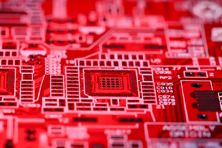
Electronics applications split cleanly into non-functional hardware (enclosures, fixtures, brackets) and functional hardware (RF, EMI, thermal, and direct-printed circuitry), and the material process map is built around that split [S1][S5].
The core technical constraint is that a PCB-style assembly needs a low-loss dielectric substrate and a conductive path, while a structural electronics part only needs geometry, surface finish, and thermal or shielding performance, so the same four material families (thermoplastic filaments, photopolymer resins, metal powders, and conductive inks) are matched to very different job lists [S2][S6].
Process-to-Material Match for Electronic Hardware
Fused Deposition Modeling (FDM) is the lowest-cost route and runs on commodity filaments such as PLA, ABS, PETG, and higher-temperature engineering thermoplastics like polycarbonate and PEEK, which makes it the default for concept enclosures, breadboard jigs, and snap-fit prototypes where dielectric performance is not on the critical path [S1][S2]. Multi Jet Fusion (MJF) and Selective Laser Sintering (SLS) use nylon-12 (PA12) and glass- or carbon-filled nylon powders, and both tolerate complex lattice geometries that would trap support material in FDM, which is why batch production of electronic casings and breadboards is migrating from machined ABS to PA12 via SLS and MJF [S1].
SLA and Carbon DLS use UV-curable resins that deliver surface roughness in the single-digit micrometer range and hold tighter tolerances than FDM, so they are the chosen path for high-definition cosmetic prototypes, thin-wall features, and water-resistant or flexible housings on foldable or wearable devices [S1]. Direct Metal Laser Sintering (DMLS) prints in stainless steel (typically 316L), aluminum (AlSi10Mg), and copper-rich alloys for brackets, mounts, RF shielding, and thermal management parts where the AM build replaces a machined or die-cast component, not a plastic one [S1][S5].
Functional Electronics: Dielectrics, Conductors, and the Bond Between Them
Functional AM electronics need a substrate with stable dielectric constant (Dk) and low loss tangent (Df) plus a conductor that can be co-deposited or post-processed, and the candidate material formats are filaments, wires, powders, pastes, sheets, and inks, with the form factor dictated by the process [S2][S6]. Newer polymer families being adapted for AM electronics include low-Dk dielectric polymers and semiconducting polymers with tunable electronic properties, both intended to replace the FR-4 substrate role in regions where a printed circuit geometry is acceptable [S1].
Multi-material additive manufacturing (MMAM) of metal-polymer hybrid structures is the active research frontier, classified into sequential deposition, simultaneous deposition, and hybrid processes, and it is explicitly motivated by the limits of single-material AM in producing parts that need both conductivity and structural compliance [S4]. Sequential deposition (print metal, then polymer, or vice versa) is the most mature route but suffers from weak interfacial bonding driven by thermal expansion mismatch and chemical incompatibility between the two phases, so designers should expect to oversize the bond area and avoid peel-loaded joints [S4]. Simultaneous deposition uses dual-extrusion or co-sintering to print both phases in one pass, which addresses the bond problem at the cost of more constrained material pairings and tighter process windows [S4]. Direct writing of conductive inks and pastes (silver, copper, carbon) onto AM polymer substrates is the route most often seen in academic demonstrators of 3D-printed antennas, sensors, and simple circuits, and the resulting trace conductivity is orders of magnitude below bulk copper, so these traces are sized for signal integrity, not power delivery [S6].
Selection Criteria, Compared Across Material Families
The decision tree is built on four criteria that map directly to spec values: dielectric behaviour (Dk, Df, or "non-functional"), electrical conductivity (bulk metal vs conductive ink vs none), minimum feature size the process can hold, and post-processing burden (support removal, sintering, plating, curing) [S1][S2][S5][S6]. For a non-functional enclosure on a 50-piece prototype run, FDM ABS or PETG scores well on cost and lead time but loses on surface finish and repeatability, while SLS PA12 wins on batch consistency and complex geometry but adds powder-handling cost; SLA resin wins on surface and tolerance but loses on thermal and impact performance relative to SLS nylon [S1].
For functional or RF hardware, the comparison shifts to DMLS metals (316L, AlSi10Mg, copper alloys) which deliver bulk-metal conductivity and shielding effectiveness at the cost of print time and post-machining, while direct-write conductive inks on AM polymer substrates deliver the lightest weight and most conformal geometry but require downstream sintering, curing, or plating to reach usable conductivity, and they are limited to low-current signal paths [S5][S6]. MMAM metal-polymer hybrids are the only route that can place a conductor and a dielectric in a single build, but process maturity is still research-stage and the supplier base is narrow, so they should be treated as a development bet rather than a production tool until the bond-strength data stabilises [S4].
Use-Case Mapping and What Each Path Is Not For
FDM, SLS, MJF, SLA, and DMLS cover roughly 80 to 90 percent of current electronics-AM work, spanning consumer devices, industrial controls, aerospace avionics, and medical electronics, with common parts being connector housings, PCB test fixtures, thermal management pieces, RF and EMI shielding, and prototype enclosures [S1][S5]. FDM is not for fine-feature RF work, and SLS/MJF nylon is not for high-temperature under-hood electronics without a thermal stabilisation step, while DMLS is not economic for cosmetic prototype shells where a 200-gram polymer part does the job [S1][S5].
Direct-write and MMAM routes are appropriate when the geometry demands a co-deposited conductor and dielectric, for example 3D-printed antennas, embedded sensors, and conformal RF structures, but they are not appropriate as a drop-in for FR-4 PCB production or for any current path above a few hundred milliamps, and designers should expect to validate conductivity, adhesion, and aging data on a per-batch basis rather than rely on a generic datasheet [S4][S6]. Reference work on AM materials for RF components explicitly flags that available conductors and dielectrics are improving but still trail bulk copper and low-loss laminates on loss tangent and trace resolution, so AM RF parts are typically demonstrators or low-volume conformal hardware, not production feed lines [S6].
Failure Modes and Process Constraints to Spec In
The recurring failure modes in AM electronics are warping and delamination at the metal-polymer interface, porosity in DMLS parts that degrades RF shielding and thermal conductivity, and inconsistent trace resistance in direct-write conductive inks caused by cure shrinkage and substrate roughness [S4][S6][S7]. Each of these is process-driven, not material-driven, which is why part orientation, infill, post-cure schedule, and plating thickness need to land on the drawing alongside the material grade, not be left to the printer operator.
For metal-polymer hybrid builds, the dominant constraint is the thermal expansion mismatch between the two phases; sequential deposition explicitly struggles with strong interfacial bonding for this reason, and the practical mitigation is mechanical interlock features (dovetails, through-holes) at the bond surface rather than relying on chemical adhesion [S4]. For DMLS shielding and thermal parts, post-process HIP or copper-infusion steps are commonly used to close residual porosity and raise effective conductivity, and these should be priced into the lead time when the spec calls for shielding effectiveness above a defined dB level [S5].
Sourcing, Standards, and Trackable Signals
Spec sheets for AM polymers in electronics should cite the exact grade (PA12 vs PA11 vs PA-CF), the build orientation, and any post-cure or annealing step, because published Dk and Df values shift noticeably between as-printed and annealed states and most vendor datasheets report only one of the two [S2][S6]. For DMLS metals, the spec should pin the alloy (316L per ASTM F3184 or AlSi10Mg per ASTM F3571 are common AM designations) plus the post-build thermal cycle, since both hardness and conductivity move with heat treatment.
Trackable signals over the next 6 to 12 months are: (1) growth of low-Dk and semiconducting polymer filament libraries aimed at AM electronics rather than generic prototyping, (2) commercialisation of dual-extrusion metal-polymer systems moving out of academic labs, and (3) wider publication of bonded-interface shear-strength data for MMAM metal-polymer parts so design allowables can replace the current "prototype-only" caveat [S1][S4][S7]. Teams specifying additive manufacturing material for electronics should also align the advanced material choice with the chemical material handling rules of the production line, since several AM resins and powders carry the same SDS obligations as the analogous bulk polymer. The automotive AM map at Additive Manufacturing Material Selection for Automotive Series and Tooling covers the alloy and process side of the same decision tree for a different end market, and the semiconductor thermal-protection spec at Choosing Thermostats for Semiconductor Process and Board-Level Protection is a useful counterpart when the AM part is being designed around a heat-load budget rather than a dielectric one.