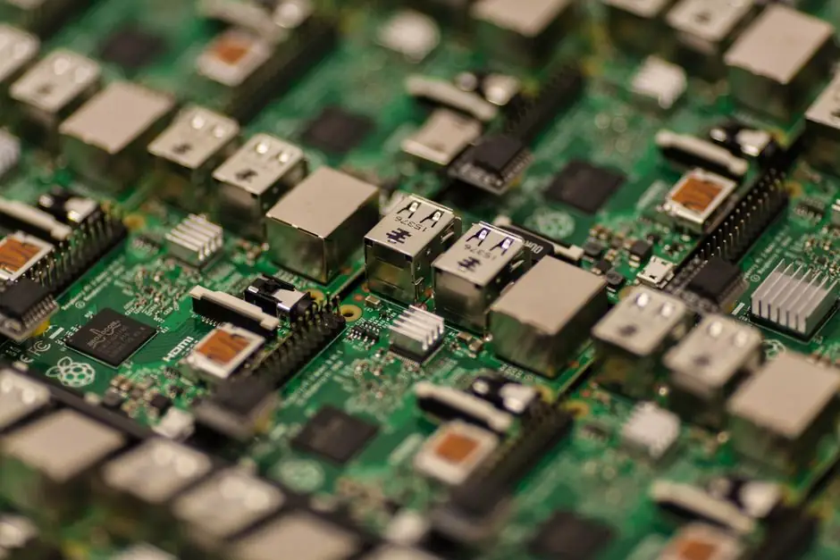
A board-level camera is a small camera module without a cover or casing, intended for OEMs that design and build their own camera housing or integrate the imager directly into a host product [S8]. In most cases board-level cameras are integrated directly into an embedded vision system or product, and a case is not required [S1][S3].
Housed cameras retain a factory enclosure, a fixed C, CS, or S-mount lens interface, and standard industrial locking connectors, which makes them a natural fit for benchtop, lab, and stand-alone machine-vision cells where the integrator does not own the mechanical design. A third niche, sometimes called a flex-frame or open-housing variant, sits between the two in size and retains some of the alignment benefits of a cased unit [S7].
Form Factor, Footprint, and Mechanical Integration
Compact board-level modules targeting embedded designs now ship in footprints around 29 mm x 29 mm x 10 mm with sub-board GPIO and interface headers, which removes the bulk of typical industrial locking connectors that alone can rival the size of a small board-level camera [S3]. Housed industrial cameras, by contrast, are built around a standardized body that accepts standard C, CS, or S-mount lenses, and the fixed lens mount becomes a hard mechanical constraint for systems that need the sensor close to the target or want non-standard optics.
Board-level cameras with no fixed lens mount let designers select optics other than the standard C, CS, or S-Mount lenses commonly used in the machine vision industry, which is attractive for laser beam profiling, biotechnology, and applications that run with no lens at all [S3]. For OEM products, the lens mount can be molded directly into the host housing, simplifying assembly and reducing part count, while a mount accessory is typically purchased separately to evaluate a board-level camera that does not ship with a mount [S3]. Designers also report that a cased model sharing the same sensor and features is often kept on the bench as a development platform while the board-level variant goes into the embedded unit [S3].
Sensor Size, Resolution, and Feature Set
Many small board-level cameras only support a few GPIO lines, low-resolution sensors, and limited on-camera features, so the transition from a cased to a board-level unit is not free: feature parity has to be checked sensor by sensor [S3]. On the other end of the range, the board-level variants of full-featured machine vision lines keep the same image-pipeline feature set as their cased siblings; one example line maintains the same 29 mm x 29 mm x 10 mm form factor across sensors from 1/3" up to 1.1", which simplifies mechanical reuse across product variants [S3].
Resolution and frame-rate pairings are dictated by the application rather than the housing: a robotic pick-and-place cell is commonly specified at 5 MP at 60 fps with 120 dB dynamic range, a medical endoscopy stream at 1080p at 30 fps with 75 dB dynamic range to keep motion blur low in confined cavities, and a traffic-monitoring channel at 4K at 24 fps with wide dynamic range around 140 dB to handle dawn and dusk plate captures [S5]. Conveyor inspection at 2 m/s needs at least 120 fps to keep motion blur under 0.5 pixels, and HDR modes, while useful where lighting fluctuates, add roughly 15 to 20 ms of processing latency on top of the imaging pipeline [S5].
Interface Protocols and Bandwidth
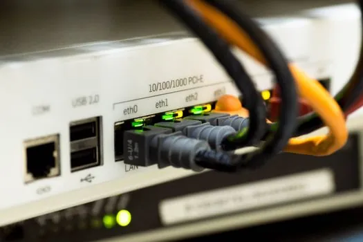
The three protocols that dominate embedded board-level integration are USB 3.1, MIPI CSI-2, and LVDS, each with a distinct bandwidth and power profile. USB 3.1 delivers 5 Gbps with plug-and-play convenience and is best kept under 3 m of cable, which suits medical imaging carts and kiosks; MIPI CSI-2 scales up to roughly 6 Gbps across 4 lanes with very low power draw and is the de facto standard for mobile and ARM-based embedded systems; LVDS trades bandwidth below 1 Gbps for strong noise immunity in electrically noisy factory environments [S5].
Latency is the deciding factor for real-time robotics, where MIPI CSI-2 with sub-5 ms end-to-end latency outperforms USB 3.1, which typically sits in the 10 to 20 ms range, so protocol choice is usually driven by deployment context: USB 3.1 for rapid prototyping, MIPI for power-constrained edge devices, and LVDS for industrial machinery near motor drives [S5]. Generic-purpose I/O is also part of the interface question, since many small board-level modules expose only a handful of GPIO lines, and bulky industrial locking connectors are a poor fit for tight embedded layouts [S3].
Thermal Management and Reliability Budget
High-resolution sensors above 12 MP draw 30 to 50 percent more power than 2 to 5 MP equivalents, and the extra heat is the dominant reliability risk in a fanless embedded chassis. Low-noise sensors drawing under 1 W while sustaining SNR above 40 dB are the typical target for confined industrial vision systems, and infrared imaging during prototyping is the practical way to confirm the design, because sustained on-sensor temperatures above 85 C accelerate sensor degradation by roughly a factor of four [S5].
Board-level modules lose the metal case that doubles as a heatsink on housed cameras, so the OEM is responsible for the thermal path to the host enclosure, the choice of sensor and ISP power profile, and the operating-point derating. The same OEM also has to manage electromagnetic compatibility from a board that no longer enjoys a sealed metal box, which is one reason EMC is listed alongside thermal management and form factor as a primary design axis for embedded vision cameras [S3].
Software Ecosystem and SDK Support
Cross-platform SDKs such as Spinnaker and Aravis abstract the hardware layer and let code move between an x86 development host and an ARM or RTOS target, which shortens the path from desktop prototype to production embedded unit. This portability matters because the same camera model may be evaluated on a workstation with a housed body, then re-spun as a board-level module for the production build, and the application code should not have to be rewritten in between [S5].
Standardized SDKs also let integrators keep their image-processing pipeline intact when swapping between MIPI CSI-2, USB 3.1, and LVDS boards from the same vendor family, which is useful for product variants that share optics and firmware but differ on connector and cable length. For deeper comparisons of related imaging hardware, see this spec decision map for image-based code readers vs laser scanners for DPM marks and this guide on color mark sensors vs standard photoelectric sensors for print registration, both of which sit alongside board-level cameras on typical packaging and print-inspection lines.
Selection Criteria and Decision Matrix
The decision between a board-level module and a housed camera can be reduced to a handful of engineering questions: who owns the enclosure, who owns the lens mount, how much power and heat can the host dissipate, what cable length and EMI environment the link has to survive, and which SDK the firmware team is willing to support. A compact comparison is useful here: housed cameras win on out-of-the-box deployment, standard C/CS/S-mount optics, and locking connectors for factory cabling; board-level cameras win on footprint, custom optics, molded-in lens mounts, and direct integration into a host product; flex-frame units win in the niche where the design needs board-level size but still wants some of the alignment and shielding of a housed body [S7][S8].
Choose a board-level camera when the OEM is designing the housing, the lens mount, or the sensor-to-target geometry itself, when the chassis is space-constrained and fanless, and when the chosen protocol is MIPI CSI-2 or LVDS rather than USB 3.1 [S5]. Choose a housed camera when the integration is a stand-alone machine-vision cell, the optical path is standard, the cabling crosses a factory floor with locking connectors, and the firmware team wants the SDK to work the same way on a lab bench and on the line [S3]. For industrial vision builds where the camera and the product are the same physical assembly, a board-level module from a line that exposes the same form factor across multiple sensors is the lower-risk path, because it preserves the imaging pipeline and the SDK contract while freeing the mechanical design [S3].
Trackable signals to watch over the next sourcing cycle: the spread of MIPI CSI-2 into higher-lane-count sensor modules beyond the current 4-lane, 6 Gbps ceiling, vendor disclosures of on-sensor temperature rise under sustained load in board-level SKUs, and SDK release notes that confirm parity between cased and board-level variants of the same sensor family.
For component-level specifications, see embedded part, automatic level, and infrared level.