Selection pivots on three hard constraints: required electrical conductivity, joint method (solderability, bonding, plating adhesion), and operating environment (thermal cycling, EMI exposure, flexure). The downstream use case — PCB traces, busbars, EMI/RFI shielding tape, or heat-spreader foil — dictates which form is fit, and most procurement failures trace back to choosing a construction-grade temper for an electronics flexure duty or vice versa.
Grade, Temper, and Purity Reference
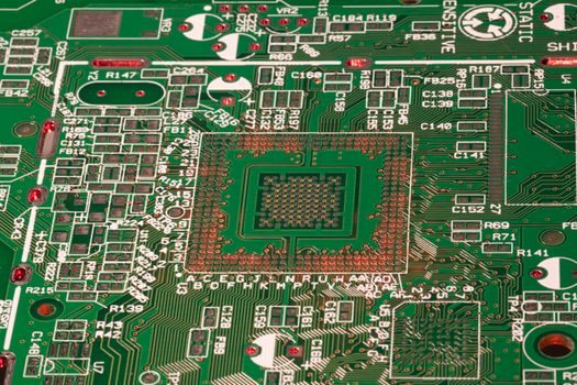
For PCB inner-layer and outer-layer foil, electrodeposited copper is the de facto standard, with typical foil thicknesses from 9 µm (for fine-line consumer boards) up to 70 µm (for power electronics), and surface roughness Rz values engineered separately on the drum side and the matte side to control adhesion to the dielectric [S1].
C11000 ETP (min 99.90% Cu, with intentionally retained oxygen) is the lowest-cost electronic-grade wrought form and remains the default for busbars, ground bars, and rolled sheet used in enclosures, where its minimum 100% IACS conductivity and good formability outweigh its hydrogen-embrittlement vulnerability at high-temperature brazing [S1]. C10100 OFE (min 99.99% Cu, ≤5 ppm oxygen) is reserved for high-vacuum tube anodes, cryogenic conductors, and sputtering targets where oxygen inclusion would poison the application, and is supplied with a guaranteed 101% IACS minimum conductivity [S1].
Forms Used in Electronics Manufacturing
The four forms map to discrete product families. ED copper foil (0.009–0.070 mm) is laminated to FR-4 or polyimide prepreg to build rigid and flex PCBs, and is the same product family that gets surface-treated with a nodular copper or zinc micro-roughened layer to anchor to the resin [S1]. Rolled annealed (RA) copper foil (1/4 hard to full hard, 0.010–0.105 mm) is the foil of choice for flexible circuits, antenna traces, and EMI shielding layers where repeated flexure would crack an as-deposited foil [S1].
Wrought C11000/C12200 plate, bar, and busbar (typically 3–25 mm thick) feed machined or stamped power-distribution parts, RF ground planes, and chassis components. Converted foil products — conductive copper foil tapes, conductive cloth with copper-nickel plating, and nano-carbon copper composite foils — are the EMI/thermal management family supplied by specialty converters and targeted at consumer device shielding [S2]. These converters ship product lines including copper foil tape (LZ/DY series), aluminum foil tape, conductive cloth tape, conductive sponge, nano carbon copper foil, and graphene heat dissipation film, sold into mobile terminal R&D, battery pack, and consumer electronics assembly lines [S2].
Selection Criteria: Conductivity vs Solderability vs Flexure
The first decision is whether the part is a current-carrying conductor or a thermal/EMI-management element. For current-carrying PCB layers and busbars, C11000 ETP or ED foil (≥100% IACS) is mandatory because even a 1% conductivity loss becomes a thermal-rise penalty in dense layouts. For shielding and heat-spreading, a slightly lower-conductivity form (C12200, or ED foil with the matte surface pre-treated) is acceptable when the gain is better adhesion to a PSA or thermal interface material [S2].
The second decision is the joining process. ETP will hydrogen-embrittle if you braze it above ~400 °C in a reducing atmosphere; switch to C12200 DHP or C10100 OFE for those joints. The third decision is mechanical duty: a part that flexes in service (flex PCB, hinge, foldable display) must specify RA temper foil with a controlled yield-strength window, never hard-rolled ETP. For a more complete map of copper grades used outside electronics — plumbing, roofing, refrigeration — see the construction-grade copper selection reference. For the basic metallurgy behind these CDA designations, the copper material encyclopedia entry gives the full UNS/temper cross-reference.
Comparison of the Four Electronics-Grade Forms
Lining the four principal forms against decision criteria gives a working selection grid.
The key trade-off is that no single form is best on all four axes. ETP wins on cost and conductivity but loses on embrittlement; OFE wins on embrittlement and conductivity but loses on cost; DHP wins on embrittlement and brazing behavior at modest conductivity; ED foil wins on thinness and laminate integration at the cost of flexure endurance unless it is rolled-annealed after deposition.
EMI Shielding and Thermal Management Converted Products
For shielding and heat-spreading duty, the copper form is often delivered as a converted laminate: copper foil with conductive adhesive, copper-nickel plated woven cloth, or copper-clad graphene film. Specialty converters serving the mobile-device and battery-pack supply chain — including suppliers that list Foxconn, BYD, ZTE, Huawei, OPPO, VIVO, and Amazon among their end customers — produce copper foil tape (LZ/DY series), aluminum foil tape, conductive cloth tape, conductive sponge, and nano-carbon copper foil grades specifically for EMI and thermal interface use [S2].
Selection in this family comes down to surface resistivity (Ω/sq), z-axis thermal conductivity (W/m·K), adhesive chemistry (acrylic, silicone, or no-substrate), and total thickness with or without carrier film. Typical EMI copper foil tape runs 0.035–0.070 mm foil with 0.030–0.050 mm conductive adhesive, surface resistivity in the low milliohm/sq range, and is rated for continuous operating temperatures up to ~120 °C with acrylic adhesive or ~200 °C with silicone [S2]. For thermal-only duty, a graphene heat dissipation film or a no-substrate thermal adhesive replaces the foil layer; the copper is dropped to lower cost where no EMI attenuation is needed [S2]. Comparable thermal-interface trade-offs in non-copper systems are covered in the quartz material selection reference.
Limits, Failure Modes, and What Not to Specify
The most common specification error is choosing C11000 ETP for a part that will see a hydrogen-containing reducing atmosphere above ~400 °C — the result is steam generation at the grain boundaries, micro-voiding, and brittle fracture at the joint. The second most common error is specifying hard-rolled ETP sheet for a flex circuit or hinge assembly; the as-rolled temper will work-harden and crack within thousands of cycles, and the fix is to drop to RA temper or to C12200 in the half-hard condition.
A third failure mode is using untreated ED copper foil (drum side out) for an application that requires lamination adhesion — the drum side is smooth and will delaminate. Always specify which face bonds to the dielectric and require the supplier to identify the treated matte side. A fourth, more exotic failure mode: specifying OFE for a high-vacuum application and receiving ETP mislabeled as OFE; the only practical defense is an incoming oxygen-content test or a third-party UNS certification on each heat of material.
Verification, Standards, and Sourcing
The governing references for electronics-grade copper are the UNS/CDA designation system (C11000, C10100, C12200), ASTM B49 (drawn or rolled rod/bar for electrical use), ASTM B152 (sheet and strip), and IPC-4562 for electrodeposited copper foil used in PCB manufacture. The foil surface-roughness, mass-per-unit-area, and purity windows in IPC-4562 are what most laminate shops actually enforce on incoming ED foil [S1].
For the related downstream process — printed circuit board stackup and trace impedance — the additive manufacturing material reference covers the metallization chemistry used in advanced PCB builds. Trackable signals for the next six months: any IPC-4562 revision activity on treated-foil nodularity limits; any tightening of EU RoHS exemptions covering copper-alloy lead-bearing grades in consumer electronics; and converter-side announcements on nano-carbon copper foil and graphene-copper hybrid films moving from prototype to volume shipment [S2].