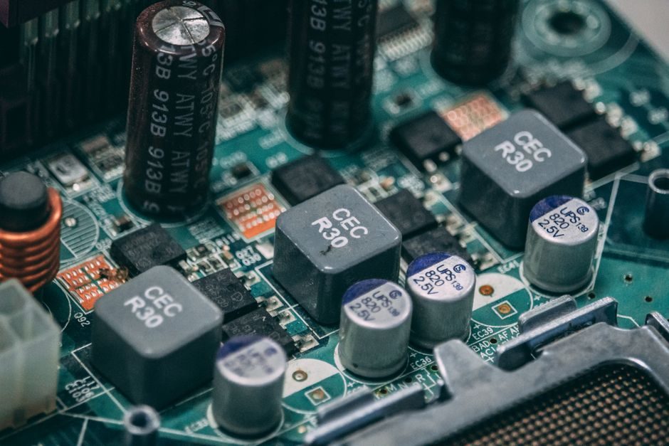
On a modern consumer or server CPU, the all-in landed cost is dominated by four cost stacks: the blank 300 mm silicon wafer, the photolithography cell (dominated by ASML EUV scanners), the back-end packaging line, and final test. The wafer itself is the single largest variable input, but the lithography, packaging, and test steps together routinely exceed wafer cost on 5 nm and 3 nm nodes [S5][S6].
This breakdown applies to x86 server parts (Xeon, EPYC), mobile SoCs and high-end client CPUs alike; cost structure varies by node, die size and packaging scheme (monolithic, chiplet, or 3D-stacked) [S4][S7].
Silicon Wafer: Substrate Cost and Diameter Choice
The starting substrate is electronic-grade silicon refined to 99.9999% purity, pulled into ingots and sliced into 300 mm wafers, the current industry standard for advanced-node CPU production [S5]. Larger diameter wafers raise die-per-wafer output and amortize fixed photolithography cost across more units, which is the main economic reason every leading-edge fab is built around 300 mm tooling rather than the older 200 mm lines [S4].
Wafer cost is the most-cited line item but rarely the largest on advanced nodes. Process step count (hundreds of lithography, etch, deposition and CMP steps) is the bigger driver of cycle time and capex depreciation per die [S5][S6]. For a typical 300 mm wafer, a chipmaker's internal wafer price is a closely held figure; what the public can verify is that defect density, not raw silicon, is what kills die yield at 3 nm and below.
Photolithography and EUV Scanners
Photolithography transfers the circuit pattern from a mask onto a photoresist-coated wafer using light. Leading-edge CPUs now rely on Extreme Ultraviolet (EUV) lithography at 13.5 nm wavelength, which is what enables sub-7 nm feature sizes and the current 2 nm / 18A generation [S5][S6]. An EUV scanner is the single most expensive tool in a fab, with each system priced well above USD 100 million, and a leading-edge fab requires multiple such units in parallel.
EUV throughput is still lower than deep-UV (DUV) by roughly a factor of two to three, so the cost-per-wafer-pass is materially higher and EUV layer count (currently in the low double digits per CPU) is a direct lever on die cost [S6]. High-NA EUV, the next-generation optics upgrade, is now being installed in volume and will raise throughput and resolution trade-offs in the 2026-2028 window [S5].
Transistor Architecture: From FinFET to GAA
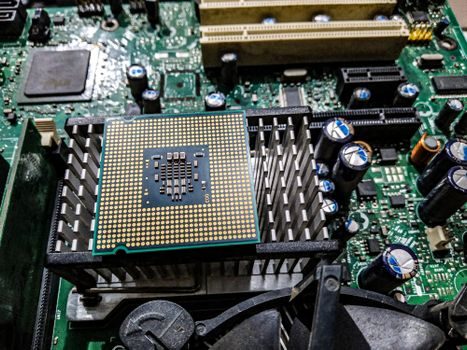
Process node shrinks have moved from 0.5 µm, through 0.35 µm, 0.25 µm, 0.18 µm and 0.13 µm, down to the current 5 nm, 3 nm and 2 nm / 18A production points, with mainstream parts now well below 10 nm [S2][S3][S5]. Each shrink roughly doubles transistor density and cuts switching power at constant performance, which is the engineering reason for the migration.
At 3 nm and below, the transistor has changed structure: the planar and FinFET layouts are being replaced by Gate-All-Around (GAA) architectures, also called nanosheet FETs, which give better short-channel control at sub-3 nm gate lengths [S5]. The newer GAA stack carries more deposition and etch steps per layer, which is one structural reason why per-die cost has not fallen as fast as transistor counts have risen.
Wafer Sort, Die Sort and Known-Good-Die
After front-end processing, the wafer is electrically probed (wafer sort) to identify functional dies, and defective cores are discarded before singulation [S4]. This step gates downstream cost: every defective die that escapes to packaging costs the full packaging budget, so aggressive wafer sort is mandatory on advanced nodes where the marginal die is profitable.
Yield is the lever that determines effective cost-per-good-die, not list wafer price.
Advanced Packaging: FCBGA, Chiplets and 3D Stacks
Once known-good dies are available, they move to back-end packaging, which is now a larger share of total cost than it was a decade ago. Common advanced packaging formats include FCBGA (Flip-Chip Ball Grid Array) for most CPUs, plus chiplet-based multi-die interconnect and 3D stacking (TSV-based) for high-bandwidth memory and compute tiles [S7].
Packaging is no longer just a protective shell: it sets signal integrity, power delivery and thermal performance. For chiplet and 3D parts, the silicon interposer, hybrid bonding or CoWoS-style carrier adds a new substrate line item on top of the FCBGA substrate and solder balls, and is the single fastest-growing line on a modern CPU BOM [S7]. The packaging share of total cost is why the rare earth and substrate cost lines in a 2026 BOM have become a board-level talking point.
Final Test, Burn-In and Quality Stack
Final test is the last gate before shipment: each packaged CPU is exercised across voltage and frequency corners, with binning (sorting parts into speed grades) and burn-in on premium server SKUs [S4]. For a Xeon-class server CPU, extended burn-in and platform-level validation can add days to cycle time and a measurable per-unit cost, which is one reason server SKU ASPs are several times client SKUs.
Yield loss at final test, plus warranty reserve for field failures, plus the platform-validation cost on reference boards, all sit on top of the wafer + packaging stack. For comparison, a GPU manufacturing cost breakdown runs the same four-bucket model, but the GPU back-end share is heavier because HBM stacking and large interposers consume more of the total BOM.
What This Means for Sourcing and Cost Engineering
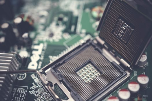
For an industrial buyer or system integrator, the practical takeaway is that CPU cost is driven by node, die size, packaging type and yield, not by the wafer line item alone. A larger die at the same node costs more because defect-density kills more units; a chiplet design at a newer node can cost less than a monolithic die at the older node once packaging is included. [S1]
Trackable signals to watch: per-wafer EUV layer count disclosure, foundry capex on High-NA EUV, and any move from FCBGA toward hybrid bonding in volume. For broader factory-floor context, the same cost-stack logic shows up in industrial control hardware; see this 2026 CPU and PLC instrumentation spec map for the control-side analog.
For component-level specifications, see additive manufacturing material, pressure transmitter, and flow meter.
For related coverage, see Best Filling Machine for Pulp and Paper: Liquid, Powder and Slurry Spec Bands.