Every DRAM cell is one transistor plus one capacitor, and getting both to shrink together is the entire problem of DRAM scaling [S2]. The full front-end flow runs through ISO area etch, buried wordlines, bitline and contact, storage node contact, capacitor etch with mesh spacer, and capacitor plate formation, with each step gated by a different metrology target [S2].
That process is the substrate for High Bandwidth Memory (HBM), the stacked-DRAM product from SK Hynix, Samsung and Micron that supplies Nvidia GPU bandwidth for AI training and inference [S3]. For an engineer sourcing equipment against that flow, the tool-to-step map and the 2026 sourcing logic are the right frame; the broader wafer fab equipment process map carries the cross-node comparison.
Step 1: Active Area and Shallow Trench Isolation
The flow starts on a lightly p-doped silicon wafer. A silicon nitride (SiN) cap plus oxide stack is deposited, a photolithography mask exposes the field, and plasma etch cuts shallow trenches, the shallow trench isolation (STI) that electrically separates neighbouring transistors [S3]. Each halogen precursor line into the etch chamber is metered by a flow meter to keep the etch chemistry on its recipe. Trenches are then refilled with CVD oxide to act as the inter-device dielectric; CVD is one of the less precise deposition modes, so overburden planarisation typically follows before the cell array is built [S3].
This STI quality is non-negotiable for every downstream step: leakage between adjacent cells and bitline-to-wordline parasitic capacitance are both seeded here. As lateral transistor CD shrinks toward 10 nm, the vertical etch profile and its wafer-uniformity must be measured with FIB-prepared cross-sections, not legacy 2D top-down SEM, per current metrology guidance [S2].
Step 2: Buried Wordline, Bitline and Storage Node Contact
With the active area isolated, the access transistor is recessed and a buried wordline (often a metal gate such as W/TiN wrapped in a high-k/work-function stack) is formed inside the groove, replacing the older planar wordline to free 4F² cell area [S3]. Source/drain epi is grown selectively on the exposed silicon, then a storage-node contact (SNCT) lands the capacitor landing pad, and a bitline (BL) contact is patterned on the complementary side, separated by a self-aligned air-gap or nitride spacer [S3].
The buried wordline pitch is the single number that defines the cell density in current 1a/1b/1c nodes. TEM cross-section is the only technique that resolves the recess depth, gate-dielectric thickness and BL-to-SNCT short-margin simultaneously [S2]. For sourcing, the metrology-side reference frame is the same one used in the broader wafer fab equipment tool stack article, where etch and deposition tool generations are compared node-on-node.
Step 3: Capacitor Etch, Mesh Spacer and High-k Dielectric
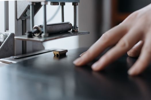
The capacitor pillar (SNCT) is then shaped into a tall cylinder or pillar to maximise surface area, the only knob left once the lateral CD is fixed. A mesh spacer etch defines a high-aspect-ratio sleeve, and a high-k dielectric stack — typically ZrO₂-based films in leading nodes — is conformally deposited before the top electrode (TiN) plates the cell [S2]. Chamber pressure during this ALD step is closed-loop controlled through a pressure transmitter, since the sub-2 nm film uniformity budget cannot absorb a precursor partial-pressure excursion.
Capacitance retention is the gate item: as the lateral CD shrinks, surface area is preserved by going taller and thinner, but thinner high-k films leak more, and the process window collapses. EDS characterisation of the Zr/O/N distribution in these stacks is therefore now standard, with newer detectors delivering at least 2× greater collection efficiency than previous generations, reducing electron-beam damage artefacts on these beam-sensitive films [S2].
Step 4: Capacitor Plate, Interconnect, and Final Test Mode Selection
A TiN top plate is deposited, the array is interconnected, back-end-of-line (BEOL) metal layers and pads are built, and the wafer is probed. Older control-mode selection (2CAS/1WE vs 1CAS/2WE) was once finalised at the very last bond step: a gold wire from a dedicated pad to the ground lead was bonded or omitted to set the device's read/write control type, deliberately leaving that decision to the final step so a single wafer lot could be re-targeted to either customer interface [S1].
That same principle — defer mode selection to the final fab step for yield-mix flexibility — still echoes in modern HBM stack configuration, where the base DRAM die and the logic die are tested at known-good-die stage before TSV-stacking. Final metal/pad lithography remains the cheapest place to convert a wafer from one customer bin to another.
Step 5: HBM Stacking and 2026 Equipment Loadout
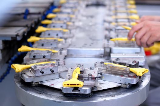
DRAM wafers are thinned, through-silicon vias (TSVs) are etched and metallised, and multiple thinned DRAM dies are bonded to a logic die using thermocompression bonding with micro-bumps, then over-moulded. The vacuum hold-down that pins each thinned die to the carrier during bonding is switched by an industrial valve manifold, since a single sticky valve on that line can scrap a full 12-Hi stack. SK Hynix, Samsung and Micron all sell variants of this stack for AI accelerators, and the HBM3E/HBM4 generations are the line items that actually decide HBM scrap cost [S3].
For tool sourcing, the DRAM front-end (etch + CVD + ALD) and the HBM back-end (wafer thinning, TSV reveal, TC bonder, underfill, mould-grind) are bought as two separate capex lines. A clean way to think about the 2026 back-end automation loadout is to compare it against the general chip-packaging smart-manufacturing stack, where AOI, robotics and digital-twin integration levels are now the differentiators between Tier 1 and Tier 2 OSATs [S3].
Comparison: DRAM Process Options and Sourcing Levers
The realistic decision axes in 2026 are: lateral CD roadmap (sub-10 nm D1z/D1a vs older D1y), capacitor architecture (cylinder vs pillar vs new 3D stack), dielectric family (ZrO₂-based high-k vs emerging higher-k), and HBM stack height (8-Hi/12-Hi/16-Hi). On metrology, TEM-with-FIB cross-section plus next-gen EDS is now the baseline for capacitor process control, while conventional top-down SEM is acceptable for STI/wordline CDs above ~12 nm [S2].
On equipment, etch and deposition intensity per wafer rises sharply at D1a and beyond; Lam Research, ASML (EUV/ArF immersion) and applied materials suppliers have all publicly framed patterning + etch + deposition as the three co-equal scaling levers for DRAM [S5]. The trade-off is direct: the more aggressive the node, the higher the TEM metrology sample volume, the tighter the cell-capacitance tolerance, and the higher the scrap cost if any of the six core steps drifts out of its process window [S2].
Failure Modes, Constraints and Standards
Three failure modes dominate DRAM yield loss. First, BL-to-SNCT short, caused by spacer thinning or contact misalignment; second, capacitor leakage, driven by high-k film non-uniformity at the sub-2 nm dielectric regime; third, TSV reveal defects in HBM, caused by thinning-grinding stress. Each is a process problem, not a design problem, and each is detected at a different metrology station [S2].
The single most cited industry constraint is refresh interval: DRAM cells lose charge on a millisecond timescale and must be recharged periodically, which is the entire reason DRAM is "dynamic" and why it cannot be made non-volatile without a new cell architecture [S4]. Wafer-scale uniformity targets are typically specified in angstrom-level film-thickness control, set fab-by-fab; cross-vendor process standards are largely internal rather than IEC/ISO-mandated for this layer.
Signals to Track Next
Two specific signals are worth watching through the rest of 2026: the first HBM4 12-Hi/16-Hi ramp announcements from SK Hynix, Samsung and Micron, which will pull DRAM wafer starts up; and the first commercial ALD tools qualified for sub-1.5 nm high-k capacitor dielectrics, which will decide whether D1a yields stabilise at the end of 2026 or slip into 2027. The equipment side of that ramp will track the chip packaging smart-manufacturing AOI and digital-twin stack modernisation pace at the leading OSATs. [S1]