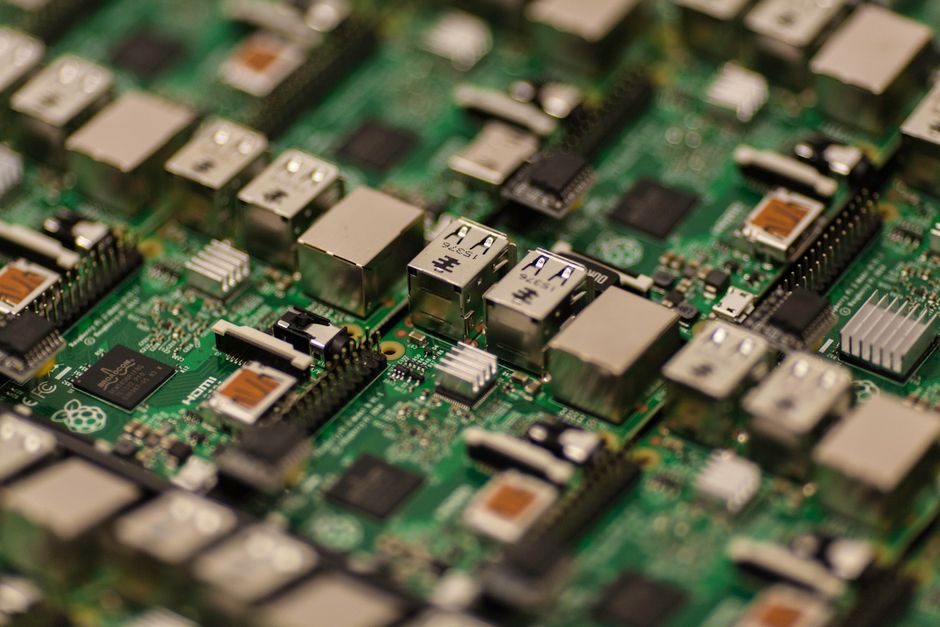
Embedded part selection is a 4-axis problem: MCU class (8/16/32-bit), clock speed, on-chip memory (Flash/RAM), and peripheral mix (I/O, ADC channels, comms). Most field decisions narrow to the smallest part that meets the I/O and protocol envelope, then verify against temperature grade, package and long-term supply [S1].
Buyers on the industrial side typically evaluate 8-bit parts for sub-USD 2 sensor nodes, 16-bit parts for motor control with PWM and quadrature decoding, and 32-bit ARM Cortex-M0/M3/M4/M7 parts when the application carries an RTOS, Ethernet, or a graphical HMI [S1]. Lead time, tool-chain maturity, and lifecycle status (active vs NRND) decide the final short list.
MCU Class vs Application Envelope
8-bit MCUs (e.g. PIC, 8051, ATmega class) typically run at 4–20 MHz, ship with 1–64 KB Flash, 64 B–4 KB RAM, and 6–32 GPIO; they fit coin-cell sensor nodes, simple PWM drivers and low-cost replacement of discrete logic [S1].
16-bit parts (MSP430, PIC24, dsPIC) deliver 16–25 MHz core clocks, 2–128 KB Flash, 0.5–8 KB RAM, integrated 10/12-bit ADC up to 200 ksamples/s, and on-chip op-amps — the sweet spot for metering and BLDC commutation [S1].
32-bit ARM Cortex-M parts span 50–600 MHz, 16 KB–2 MB Flash, 4–512 KB RAM, and 20–200+ GPIO; they are the default pick when TCP/IP, USB, CAN-FD, or an LVGL/HMI stack is in scope [S1]. For factory-floor node design, see the embedded part reference for typical 8/16/32-bit envelope and package data.
Memory Sizing Rules of Thumb
Flash headroom of 20–30% over compiled code size is the usual engineering rule; below that, code updates become risky and linker padding eats the gain [S1].
RAM sizing follows three buckets: application variables + RTOS/TCP stack (if any) + stack/heap headroom. A bare-metal Cortex-M0 application with a Modbus slave typically fits in 8–16 KB Flash and 2–4 KB RAM; adding LwIP TCP/IP pushes the same design to 64–128 KB Flash and 16–32 KB RAM [S1].
EEPROM endurance is 100 k–1 M write/erase cycles for most on-chip EEPROM and 10 k–100 k for Flash-emulated EEPROM; data-logger designs above that rate need an external FRAM (e.g. SPI FM25Vxx) or a wear-levelling layer [S1].
Peripheral and Comms Checklist
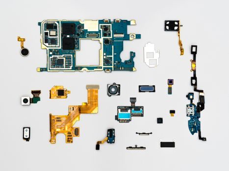
Count GPIOs after reserving pins for: debug (SWD/JTAG = 2–5 pins), boot mode (1–2 pins), crystal (2 pins if no internal oscillator), and one UART for the bootloader; a 32-pin package typically nets 18–22 usable GPIO once these are booked [S1].
ADC resolution and speed are separate specs: 12-bit at 1 Msample/s is common on Cortex-M3/M4, 16-bit sigma-delta on dedicated metrology MCUs (MSP430i20xx) hits 2–4 ksps with effective ENOB above 14 bits [S1].
Comms selection follows the wire: UART (RS-232/RS-485) for legacy and Modbus, SPI up to 30–50 MHz for short PCB runs, I2C 100/400/1000 kHz (Standard/Fast/Fast+) for sensor buses, CAN 1 Mbit/s or CAN-FD 2–5 Mbit/s for vehicle and industrial machinery [S1].
Power, Temperature and Package Constraints
Active current scales with MHz and peripheral count: a Cortex-M0 at 16 MHz draws 1–3 mA active, a Cortex-M4 at 100 MHz with all peripherals on draws 15–30 mA, and a Cortex-M7 at 400 MHz with cache active can clear 80–120 mA — sleep current is the more honest battery-life number and ranges from 50 nA (deep sleep, RTC running) to 10–50 µA (standby) on most modern parts [S1].
Industrial temperature grade (-40 °C to +85 °C) is the default; -40 °C to +125 °C (AEC-Q100 Grade 1 for road vehicles, or extended-industrial) costs 1.3–2× the commercial-grade unit price and is mandatory for under-hood, outdoor enclosure, and oilfield sensor designs [S1].
Package choice locks PCB: QFN/QFP 0.4–0.8 mm pitch needs reflow and 4-layer routing, SOIC/TSSOP 1.27 mm pitch hand-solders, and BGA (0.5–0.8 mm pitch) is essentially reflow-only with X-ray inspection for production. A 32-pin QFN at 5×5 mm shrinks board area versus 32-pin QFP at 7×7 mm by roughly 50% [S1].
Tool-Chain, Lifecycle and Sourcing Filters

Tool-chain maturity is a hidden cost: GCC + OpenOCD + GDB is free but ramp-up is real; vendor IDEs (STM32CubeIDE, MPLAB X, MCUXpresso, ESP-IDF) shorten time-to-blink but bind firmware to a vendor SDK and middleware stack. Library quality (HAL vs LL vs register) drives RAM overhead by 10–30% [S1].
Lifecycle status trumps spec: a part marked NRND (Not Recommended for New Designs) or with last-time-buy dates inside the design window disqualifies the BOM. Field life of industrial equipment is 10–15 years, so an active roadmap with 10+ year supply commitment is the practical gate [S1].
For robotics, automotive chassis controllers, and hydraulic-line sensor stacks where the embedded part sits next to a pressure transmitter on the same board, dual-source with pin-compatible second-source (e.g. STM32F4 ↔ GD32F4, ATSAM ↔ SAMD) de-risks allocation. A 20–30% buffer on production orders held in bonded warehouse is the common hedge against 26–40 week industrial lead times.
Decision Matrix: 8-bit vs 16-bit vs 32-bit
Compare the three classes on four buying axes: [S1]
Cost per unit: 8-bit USD 0.30–1.50, 16-bit USD 1.20–4, 32-bit Cortex-M0/M3 USD 1.50–6, Cortex-M4/M7 USD 3–15 — bare die pricing for orders above 10 kpcs [S1].
Comms fit: 8-bit covers UART/SPI/I2C; 16-bit adds CAN and USB device; 32-bit covers Ethernet, USB OTG, CAN-FD, SD card, and camera parallel ports. HMI or HMI-over-LCD projects collapse to 32-bit [S1].
Power floor: 8-bit and 16-bit dominate the <1 µA sleep envelope; 32-bit parts now offer 50–200 nA deep-sleep with RTC retention, but average active power is 5–10× higher than 16-bit at the same workload [S1].
Ecosystem: 8-bit has the deepest legacy code base, 16-bit (MSP430, dsPIC) has best-in-class analogue, 32-bit (Cortex-M) has the widest middleware, RTOS, and third-party library support [S1].
Common Failure Modes and Spec Traps
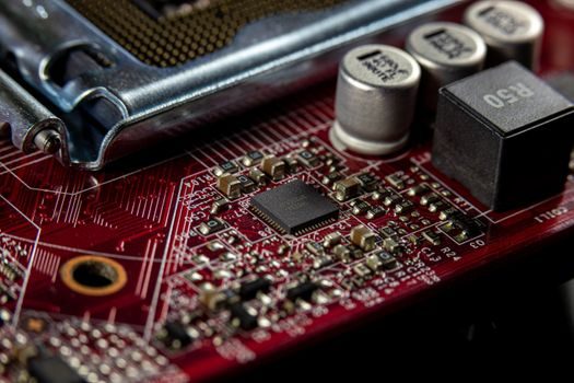
Brown-out voltage (BOR) and watchdog window (WWDG) are frequently left at defaults; industrial designs must enable BOR at the supply rail minimum and a 30–50 ms window watchdog to recover from firmware hangs in the field [S1].
ADC input impedance and source impedance together set effective ENOB: a 12-bit ADC with 1 kΩ source impedance loses roughly 1 LSB; 10 kΩ source drops 2–3 LSB and demands an input buffer. Reference-voltage stability and PCB layout (ground plane under the ADC) drive 3–5 LSB of the total error budget [S1].
EMC immunity is set by hardware, not firmware: 4-layer PCB with continuous ground plane, ferrite on supply, common-mode choke on Ethernet/PHY, and a TVS on each external connector. Firmware-based debounce and CRC only paper over a poor layout [S1].
For cable-gland, IP-rated enclosure and field-cable selection next to the embedded board, the cable gland buying guide covers the matching IP66/IP68 spec bands used in industrial nodes.
Selection Workflow You Can Reuse
Start with the I/O count: pin-budget every external chip (sensor, comms PHY, display) plus debug and boot, then add 10–15% margin. This pins the minimum package and eliminates most 8/16-bit candidates that fail on I/O [S1].
Then match comms: list the bus types and speeds, and confirm each has a dedicated peripheral on the part. A shared SPI bus with three slaves needs three CS lines and a DMA path for burst reads; this rules out 8-pin parts early [S1].
Pin the memory budget: compile a representative firmware (drivers + application + RTOS + stack) and read the .map file. The smallest part whose Flash has 20–30% headroom wins on cost and power [S1].
Finally check the supply chain: lifecycle status, second-source, 10-year roadmap, distributor stock, and 26–40 week lead time. A part that meets every spec but is in allocation is the wrong part. For new projects in 2026, Cortex-M0+/M4 from ST, NXP, Microchip, Renesas, and the GD32 second-source family are the highest-confidence pool [S1].
Track these signals over the next quarter: ARM Cortex-M85 adoption in edge-AI sensor nodes, RISC-V 32-bit parts (GD32V, ESP32-C) gaining second-source depth, and the AEC-Q100 Grade 1 cost premium for automotive-grade parts. A flow meter or pressure sensor front-end paired with a Cortex-M0+ remains the workhorse BOM for 4–20 mA + HART 7 field devices, and HART sits as FSK on the analog loop — separate from Foundation Fieldbus or PROFIBUS PA — so a 32-bit part with a dedicated UART plus a HART modem is the correct architecture, not a Foundation Fieldbus stack.