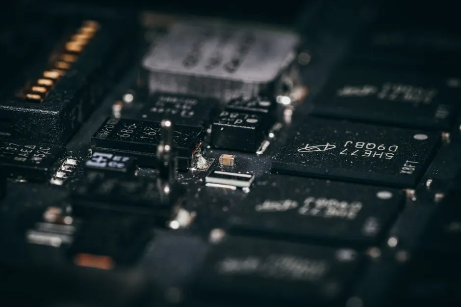
Semiconductor height measurement sits in a different resolution class from general machining: front-end processes routinely demand 0.1 µm to 1 µm vertical resolution on features from die-level step height to wafer bow, which excludes conventional 1D vernier height gauges sold for machine shops [S1].
A 1D height gauge remains the fastest tool for linear vertical checks such as thickness, depth, and step height, while a 2D height gauge adds a second axis for contour and surface profile work [S1]. For semiconductor buyers, that distinction is the starting line, not the finish line: the question is which 2D or non-contact architecture survives cleanroom thermal, vibration, and throughput constraints.
Why a Machine-Shop 1D Height Gauge Fails in a Fab
General-purpose vernier height gauges from Starrett, Mitutoyo, Brown & Sharpe, and Chesterman, even the master-grade satin-chrome 50-division vernier models widely praised by machinists [S2][S4][S5], resolve to 0.001 inch (roughly 25 µm) at best, and their cast-iron or steel bases are not engineered for granite- or kinematic-stage-level flatness over 300 mm.
Forum consensus across machinist communities is consistent: mechanical vernier and dial height gauges win on reliability because they have no batteries, no firmware, and no LCD failure modes [S2][S4][S5]. That is exactly the wrong tradeoff for a fab, where the bottleneck is resolution and thermal drift, not battery life. A digital height gauge that drifts 5 µm in a 0.5 °C cleanroom temperature swing is useless at the back-end-of-line thickness check.
For a 12 inch (300 mm) wafer, height-map uniformity budgets frequently run tighter than 5 µm total, which forces metrology away from contact mechanical probes and into optical, capacitance, or laser triangulation architectures. Plain vernier or dial gauges, even the celebrated Starrett 254 master vernier [S2], are simply not in the resolution bracket.
Resolution and Probe Type as the First Cut
Probe technology is the single biggest selection gate. For semiconductor use, three architectures dominate: chromatic confocal optical probes, laser triangulation, and capacitance probes. Each has a different sweet spot on resolution, standoff, and material reflectivity, and the wrong pairing produces misleading step-height data on polished silicon or low-k dielectric stacks.
A chromatic confocal probe typically delivers sub-micron axial resolution (often 0.01 µm to 0.05 µm) with millimeter-scale standoff, which makes it tolerant of irregular die topographies. Laser triangulation sensors trade some resolution for faster scan rates and longer standoff, useful for in-line wafer-handling robotics. Capacitance probes are the workhorse for sub-nanometer-resolution wafer-bow and thickness mapping, but they require guarded fixtures and grounded targets, which complicates fixturing on packaged parts.
Contact 1D and 2D height gauges with LVDT or glass-scale readouts are common in back-end package metrology where probe marks are acceptable, and this is where 2D contour-scanning height gauges with a motorised Y-axis earn their keep [S1]. Even there, expect to be evaluating instruments in the 0.5 µm to 2 µm resolution bracket, an order of magnitude finer than the 25 µm floor of a machinist's vernier height gauge.
Selection Criteria for 2D and Non-Contact Height Gauges
Build the spec sheet around six numbers, in this order: axial resolution, full-scale range, thermal coefficient, probe tip geometry (or optical spot size), scan-axis orthogonality, and data interface. Anything that fails on the first two items is immediately disqualified for fab work. [S4]
Axial resolution is non-negotiable. For die step height, look for at least 0.1 µm; for wafer thickness, 0.01 µm with a capacitance or optical gauge is the working minimum. Range depends on wafer size: 300 mm wafers need at least 310 mm X-axis travel, and package-level work may need 600 mm or more. Thermal coefficient of expansion for the granite or Zerodur base should be stated in parts per million per °C; general-purpose height gauge bases rarely publish this, which is itself a red flag for semiconductor use.
Probe tip geometry governs minimum feature size. Optical spot diameters of 2 µm to 10 µm are typical for confocal probes, and any spec sheet that lists only a generic "laser" without spot size is incomplete. Scan-axis orthogonality, usually stated in arcseconds or µm/m, drives the map accuracy on a 300 mm wafer. Data interface matters for in-line use: Ethernet, RS-232, or SECS/GEM is the practical minimum; isolated USB on a standalone gauge is fine only for offline QA. For the broader dimensional-metrology context, see this caliper vs micrometer selection map, which covers the resolution and error-band reasoning that transfers directly into gauge selection.
Comparison of the Main Height-Metrology Architectures
There is no single "best" architecture, only a best fit per measurement. The honest way to compare is to line them up against the four criteria that actually decide a fab buy: resolution, standoff, material compatibility, and cost of ownership. [S2]
Chromatic confocal probes: best axial resolution in its class, standoff typically 0.3 mm to 30 mm, works on transparent, polished, and rough surfaces including glass and photoresist, and sits in the mid-to-high price tier with single-point sensor heads in the several-thousand-dollar range. Laser triangulation: resolution typically 1 µm to 5 µm, standoff 10 mm to 200 mm, fast acquisition, sensitive to surface reflectivity and angle, lower cost. Capacitance probes: best resolution (sub-nanometer), very short standoff (under 1 mm), requires grounded target and guarded fixturing, mid-to-high price. Motorised 2D contact height gauge: resolution 0.5 µm to 2 µm with a glass scale, full XY travel up to 600 mm or more, leaves a probe mark, lower recurring cost.
For wafer thickness and bow, capacitance wins. For die step height and bump height, chromatic confocal or laser triangulation wins. For package lead-frame and substrate profiling, a 2D motorised contact height gauge is still the most cost-effective answer, and that is where the 1D-versus-2D distinction in [S1] actually pays off in a semiconductor-adjacent shop. For cleanroom anti-static and ESD considerations that often co-occur with these measurements, see this spec-first anti-static equipment selection guide and the sputtering target selection map for adjacent process-engineering context.
Who It Is For, and Who Should Not Buy
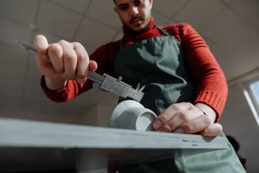
This spec path fits wafer fab process engineering, back-end package metrology labs, and OSAT (outsourced semiconductor assembly and test) QA groups that need traceable height data on structured wafers, bumped die, and leaded packages. [S1]
It does not fit general machine shops, tool rooms, or job shops buying a height gauge to lay out a 12 inch part on a surface plate. The community verdict there is durable: a used Starrett 12 inch vernier with a 50-division vernier in satin chrome [S2][S4], a 12 inch or 24 inch Brown & Sharpe or Etalon from the used market [S4][S5], or a Rabone Chesterman mechanical model [S5] will outlast any digital gauge in that environment. The economics and the resolution are simply different problems, and conflating them wastes both budget and time.
Limits, Failure Modes, and Calibration Discipline
Every architecture has a failure mode worth budgeting for. Chromatic confocal probes lose signal on highly reflective, mirror-finish metal layers at near-normal incidence; a slight tilt of 5° to 15° on the fixture is the standard workaround. Laser triangulation sensors speckle on grainy copper or aluminium bond pads, producing noisy height maps; a polarising filter or averaging filter is the usual fix. Capacitance probes drift with cable flex and require frequent zeroing, which is why the gauge controller's automatic re-zero routine matters as much as the probe spec itself. [S1]
Calibration discipline is the under-appreciated half. A height gauge on a fab floor should be supported by a regular artefact-traceable check using a step height standard (commonly a 1 µm to 100 µm certified reference) and a flatness reference. For semiconductor-spec use, look for gauges that ship with ISO 10360-style or equivalent linear-accuracy statements expressed as MPE (maximum permissible error) over the full measuring range, not just a "resolution" headline number. A 1 µm resolution sensor with 5 µm MPE is a worse buy than a 0.1 µm resolution sensor with 0.5 µm MPE, even if the headline number looks smaller. For mechanical shop buyers who never need this level of discipline, the same logic in reverse applies: a used Mitutoyo 12 inch vernier for $25 to $75 [S4] outperforms any sub-$100 digital height gauge in long-term stability.
Sourcing and Standards to Anchor the Spec
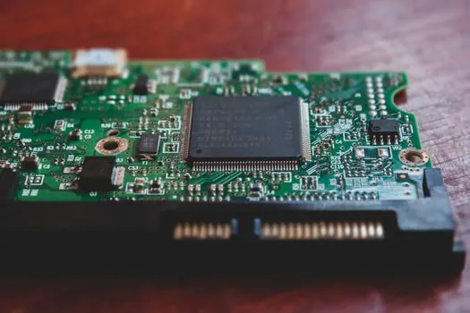
Two standards anchor semiconductor height metrology. ISO 10360 covers the acceptance and reverification test procedures for length-measuring instruments and is the correct reference for stating linear accuracy in MPE form. ISO 25178 and ISO 4287 cover surface texture parameters (Ra, Sa, and higher-order filters), which is the spec language to demand when a height map feeds into roughness or waviness reporting. [S1]
Traceability back to a national metrology institute (NIST, NPL, PTB, NIM, or equivalent) through the calibration certificate is non-negotiable for fab-grade height gauges; without it the data is informational, not auditable. For the buyers who need 1D and 2D height gauges in a non-semiconductor shop, the basic dimensional-measurement vocabulary and tolerance language in this height gauge encyclopedia entry covers the mechanical-shop context, and the thickness gauge entry covers the related single-axis instrument family used for coating and foil work. Trackable signals to watch over the next buying cycle: 2D motorised height gauges with sub-micron glass scales entering the under-$10,000 price band, and chromatic-confocal probe controllers gaining Ethernet/IP or SECS/GEM interfaces for in-line fab use.
The underlying component specifications are covered under force gauge.
