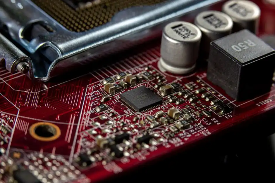
Advanced packaging lowers AI chip supply loss by splitting a large accelerator into smaller chiplets that can use different process technologies, avoiding the yield penalty of manufacturing one large defect-sensitive die.
The approach supports 2.5D and 3D integration of compute, HBM and I/O dies, but each added bond, via and interconnect introduces new opportunities for packaging yield loss [S1][S2][S4].
Why monolithic die yield constrains AI chip output
A typical AI accelerator can contain many compute, memory and I/O chiplets, with each chiplet sized within a commonly used reticle limit of 26 × 33 mm² [S1]. Dividing a processor into smaller dies reduces the area in which a single defect can scrap an entire accelerator, allowing manufacturers to salvage good chiplets instead of losing a complete large die.
Chiplet partitioning also lets designers assign functions to suitable process nodes rather than forcing logic, I/O and memory-related circuitry onto one monolithic die [S1]. Demand for chiplet integration using 2.5D and 3D advanced packaging technologies has surged, driven by the exponential growth in computing performance required for artificial intelligence and machine learning.
This strategy is not suitable where a design requires a single uninterrupted die, a fixed analog interface or a package with minimal interconnect overhead. Chiplets solve part of the yield problem, but they exchange die-level yield risk for assembly, bonding, thermal and test risks at package level [S1][S2].
Where package yield is lost
Advanced package yield depends on more than the electrical integrity of each die. It includes die warpage, fine-pitch wiring formation, bonding precision, package flatness, substrate quality, thermal control and package-level test coverage [S2][S5]. A defect in any one of these elements can reject an assembly containing several expensive compute dies and HBM stacks.
As advanced packages incorporate more chiplets, denser interconnects, and advanced bonding schemes, they introduce manufacturing complications such as die warpage, fine-pitch wiring formation, and bonding precision. Applied Materials reported uniform, void-free fill for geometries including TSVs smaller than 3 µm and deeper than a 10:1 aspect ratio, illustrating how tightly packaging process control is linked to stacking yield [S5].
Hybrid bonding raises the precision requirement because reliable bonds require exceptionally flat and uniform surfaces. Chemical mechanical planarization, or CMP, is used after TSV fill, dielectric deposition and copper-pad formation, with packaging applications generally involving thicker films, longer polish times and tighter tolerances than front-end CMP [S5].
How 2.5D and 3D packaging change supply

2.5D packaging places logic dies and HBM stacks on or near a silicon interposer, shortening the electrical path for data moving between compute and memory. A vertical HBM stack consists of DRAM dies placed beside a processor, with fine interposer wiring providing the throughput required by AI workloads [S2][S5].
3D integration places dies in three dimensions and creates direct connections between them. Synopsys identified 2.5D, 3D-IC, heterogeneous integration, fan-out wafer-level packaging and system-in-package as common advanced-packaging techniques, while the IEEE review covers 2.5D and 3D chiplet integration [S1][S4].
Why packaging capacity can still cap AI supply
Yield improvement raises the output of each packaging line, but it does not remove the capacity constraint created by the number and size of packages. AI accelerators need more compute dies, I/O dies and HBM stacks in each package, and larger packages are harder to keep flat, require stronger substrates and impose greater thermal and yield risk [S2].
Those figures show why reducing packaging yield loss is necessary but insufficient. If CoWoS lines, HBM stacks or supporting facilities remain constrained, improving defect control cannot by itself create enough finished AI accelerators [S3][S5].
Interconnect choices determine yield and energy cost

Chiplet interconnects must satisfy bandwidth density, energy efficiency, electromigration, power integrity and signal-integrity requirements [S1]. The IEEE review describes a parallel data bus with forwarded clocks as a simple architecture intended to limit power overhead, while warning that high-yield manufacturing and robust performance still require design and process co-optimization [S1].
The review also identifies Universal Chiplet Interconnect Express, or UCIe, as an important chiplet-interconnect framework [S1]. Increasing bandwidth through finer-pitch wiring does not automatically improve supply, because deposited metal fill, surface coplanarity and bonding precision must remain within process limits [S1][S5].
For AI supply planning, interconnect pitch should therefore be evaluated alongside bond yield, package flatness, thermal performance and test coverage. A nominally dense interface that raises assembly defects or power consumption may worsen the economics of finished-chip output [S1][S2].
What advanced packaging is suitable for
Advanced packaging fits AI accelerators and HPC products that require large compute arrays, high memory bandwidth and tightly coupled processor-memory interconnects. It also suits automotive, IoT and industrial modules that combine sensing, I/O, computation and memory, provided the package can meet thermal, reliability and qualification requirements [S4][S5].
It is less attractive for simple products that require very low unit cost, minimal package height or a mature ecosystem already optimized around conventional assembly. Fan-out wafer-level packaging, 2.5D, 3D-IC, heterogeneous integration and system-in-package also have different interconnect pitches, thermal burdens, manufacturing flows and cost structures, so a process family should not be selected from bandwidth claims alone [S4].
Metrics for verifying supply improvement
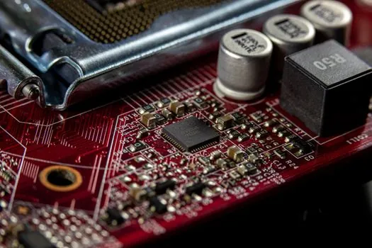
Packaging yield must be measured at die, wafer, bond, package and final-test levels, because a high probe yield can still produce low finished-package output. Useful production indicators include bonded-die yield, TSV fill defects, microbumps per die, HBM layer count, package flatness, thermal resistance and test coverage [S2][S5].
Capacity plans should also distinguish logic wafer starts from CoWoS or other package starts and from HBM stacks. The 90% CoWoS and HBM consumption estimate for the four largest designers in 2025, compared with 12% for advanced logic dies, makes component-level allocation a more useful supply signal than total wafer capacity alone [S3].
The next trackable signals are CoWoS expansion, HBM layer counts, measured package yield and defect density at TSV fill, hybrid bonding and final test. Improvement in these four areas would determine whether higher packaging yield converts into more shippable AI accelerators rather than more usable silicon waiting for assembly [S3][S5].