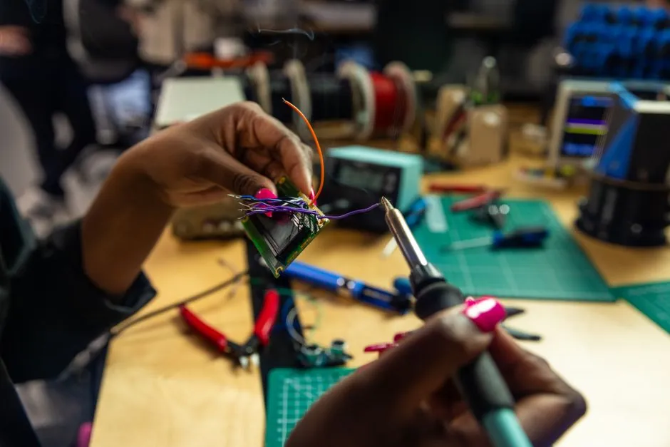
The PCB supply chain is the end-to-end path from raw laminate and copper foil through bare-board fabrication, component sourcing, surface-mount assembly, inspection, and packaged delivery, and every stage has a separate vendor set with its own lead time and risk profile [S1][S2].
Per Cognitive Market Research, the global PCB and PCBA market is projected to reach USD 78.89 billion in 2025 with a 3.7 percent CAGR, which means a single missing component or a delayed bare board can stop an entire SMT line [S2]. The chain breaks into seven linked stages, each with named stakeholders, qualification gates, and known failure modes that any sourcing engineer has to manage in parallel.
Stage 1: Design and DFM, Where the Chain Starts
The chain starts at PCB design, where electronics, mechanical, and PCB layout engineers produce a CAD database and a Bill of Materials that downstream procurement and fabrication will execute against [S4]. Design for Manufacturing (DFM) checks must be run before release, because feature sizes, copper weights, and drill tolerances all have to fall inside the fabricator's process window, otherwise yield collapses and lead time stretches [S1]. For boards that will run into the millions over a 10+ year lifecycle, a long-term sustainable component and material selection is mandatory, since product end-of-life is forced once any part goes EOL [S1].
Layout decisions made in this stage also lock in raw material choices, FR-4, CEM-1, CEM-3, polyimide, high-Tg laminate, that the fabricator then has to source against a slash sheet, with limited swap room if the preferred grade is short [S3][S4].
Stage 2: Raw Materials, Copper Foil, Laminate, Prepreg, Chemicals
PCB manufacturing draws on a wide raw-materials basket: copper-clad laminates and copper foils for the conductive layers, prepregs (resin-impregnated fiberglass) for bonding multilayer stacks, plus ferric chloride, ammonium persulfate, and copper plating solutions for etching and plating [S3][S4]. FR-4 is the workhorse substrate, with CEM-1 and CEM-3 used in lower-cost single- and double-sided builds, and polyimide specified where temperature or flex performance rules FR-4 out [S3].
Specialised inputs, silver ink, polyimide film, and precious-metal finishes, run on a much narrower supplier base, so a single allocation cut on those can halt a build that has no qualified substitute [S3]. Procurement teams therefore source from a global network concentrated in Asia, Europe, and North America, with each region offering different trade-offs on cost, lead time, and minimum order quantity [S4].
Stage 3: Bare Board Fabrication

Fabrication turns the raw laminate stack into a finished bare board through drilling, etching, electroplating, and lamination, with the output inspected against the design database before it ships to assembly [S4]. Quality control at this gate catches trace shorts, opens, and annular ring violations that would otherwise be discovered only after expensive component mounting, so an in-line AOI plus electrical test step is standard rather than optional [S4].
Lead time at this stage is set by lamination cycle time, drill stack capacity, and surface finish chemistry availability, with ENIG, HASL, and immersion tin/tin-bismuth each tied to a different chemical supply pool. In practice a 4-layer ENIG prototype commonly runs 5 to 10 working days, while a 12-layer high-Tg build with impedance control is more typical at 3 to 5 weeks, and the gap is almost entirely raw material and process-queue driven, not labour driven.
Stage 4: Component Sourcing and BOM Risk
Component sourcing is the single largest source of on-time delivery risk, because semiconductor lead times run independently of the bare-board schedule, and a single allocated part can stop kitting even when the board is on the dock [S2]. Forecasts have to be checked against the BOM for accuracy, long-lead-time parts have to be flagged, and second sources have to be qualified before the shortage shows up on the buyer's desk [S2].
JIT sourcing makes the line fast under steady conditions and extremely fragile under disruption, so most EMS providers now layer a safety stock on top of JIT for parts with allocation risk, with the exact stock level set by lead time variance and demand volume. The semiconductor and passive-component networks that feed the PCBA line are themselves multi-tier, with foundry capacity, wafer substrate, and package/test capacity each on a different clock.
Stage 5: SMT Assembly, Kitting, and the SMT Line
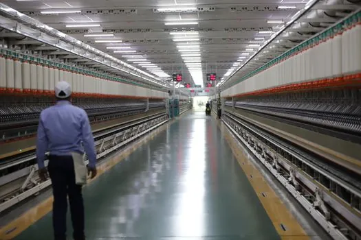
Assembly begins with solder paste printing, followed by high-speed pick-and-place of components, reflow soldering, and either wave or selective soldering for any through-hole content [S4]. Modern SMT lines run fast enough that a single mis-kitted reel can idle the whole line, so the kitting accuracy has to be verified against the BOM before the first paste deposit, not after the first placement error stops production [S2].
Packaging for components also matters more than most buyers expect, since PCBs and parts need moisture-barrier bags (MBB) with humidity indicator cards and ESD-protective packaging to survive storage and shipping without delamination or static damage [S3]. This packaging layer is part of the chain, not a side issue, and a missed MBB step on a moisture-sensitive part can produce reflow cracking that only shows up at the final test gate.
Stage 6: Inspection, Test, and Qualification
Inspection layers are stacked, with solder paste inspection (SPI) before reflow, automated optical inspection (AOI) after reflow, and X-ray inspection on BGAs and QFNs where the joint is hidden under the package [S4][S5]. Strong inspection processes support consistent quality, with industry data showing high first-pass yield levels when testing and process control are maintained, so the inspection cost is paid back by lower rework and RMA exposure [S2].
Final electrical test, in-circuit test (ICT) or flying probe, plus functional test, gates shipment to the OEM, and failures here are tracked back through the chain to find whether the root cause is the bare board, the component lot, or the process. For higher-reliability programs, qualification adds thermal cycling, vibration, and sometimes burn-in, and the cost of that gating is justified by the cost of a field failure.
Stage 7: Packaging, Storage, and Delivery

Once the board passes test, the chain moves into anti-static packaging, dunnage, cartonisation, and shipping, with storage conditions and humidity control maintained all the way to the OEM's incoming dock [S3][S5]. Supply chain management at this stage covers safe storage of the finished PCBA, packaging, shipping, and invoicing, all of which sit on the back end of the chain and are easy to underestimate until a sea-freight delay idles an OEM's assembly line [S5].
Logistics is the chain's stress point, since most manufacturers, including PCB shops, run a JIT model that is highly vulnerable to port congestion, container shortages, and customs holds, and a single delayed air-freight slot can reroute a build to a more expensive transport mode at short notice [S3]. For a deeper look at how material flow planning decisions like this one cascade into downstream factory throughput, see the analysis of LiDAR sensor capacity planning: ramp evidence, calibration bottlenecks, and the 2026 EMS.
Who the Chain Is For, and Where It Breaks
The PCB supply chain is engineered for OEMs and EMS providers that need repeatable, audited, multi-tier sourcing with full BOM traceability, and it is not built for buyers chasing a single prototype on a tight calendar without a qualified vendor list. It works best when design, procurement, and quality are wired into a single feedback loop, and it breaks fastest where one of those three functions is siloed off the other two [S1][S2].
Green or sustainable sourcing adds a parallel constraint on the same chain, requiring design, sourcing, manufacturing, and delivery choices that minimise eco-footprint across the full material flow rather than optimising cost at one stage only [S6]. The cost of that sustainability audit is real, but it is also the lever that large OEM customers are starting to mandate in their supplier qualification audits, so a shop that cannot document it will be cut from approved-vendor lists on the next refresh cycle.
How the Stages Stack Against Selection Criteria
Comparing the major stages against decision criteria makes the trade-offs explicit: design controls cost and lead time but cannot fix a missing component; raw material sourcing controls MOQ and price but is exposed to single-supplier risk; fabrication controls bare-board quality but not assembly yield; component sourcing controls on-time delivery but not final test yield; SMT controls throughput and rework cost; inspection controls field failure rate; logistics controls total landed cost and schedule [S1][S2][S4].
For a process engineer, the practical implication is that you do not pick a single supplier to optimise one stage, you pick a chain architecture where each stage has at least one qualified alternate and where the feedback loops from inspection, test, and field returns feed back into design and procurement. That architecture is the difference between a chain that absorbs a 12-week IC shortage and one that misses its customer commit on the first week of the allocation.
Standards, Sourcing, and Trackable Signals
Material and process standards that govern this chain include IPC-A-600 for bare-board acceptance, IPC-A-610 for assembled board acceptance, IPC-6012 for rigid board performance, and J-STD-033 for moisture-sensitive handling, each of which sets a documented pass/fail line that the inspection stages enforce. UL 796 covers PCB flammability rating, and RoHS plus REACH govern the material chemistry list that procurement must screen against before any new part or laminate is released. [S2]
Trackable signals to watch on the next reporting cycle: the PCBA market size update for 2025 to 2026 against the USD 78.89 billion 2025 baseline [S2], allocation status on high-density BGAs and high-layer-count substrates, and the spread between ENIG and immersion tin chemical lead times as a leading indicator of bare-board capacity. For buyers building a sourcing playbook, the most useful internal metric is first-pass yield at ICT plus on-time delivery to the OEM dock, tracked weekly against the BOM's top 20 long-lead-time parts, with the related reference for shop-floor components and fasteners laid out in Industrial Fasteners Market 2026: Manufacturer Share, Material Split, and Sourcing Map.
For the relevant spec sheets and selection criteria, see power supply, dc power supply, and switching power supply.