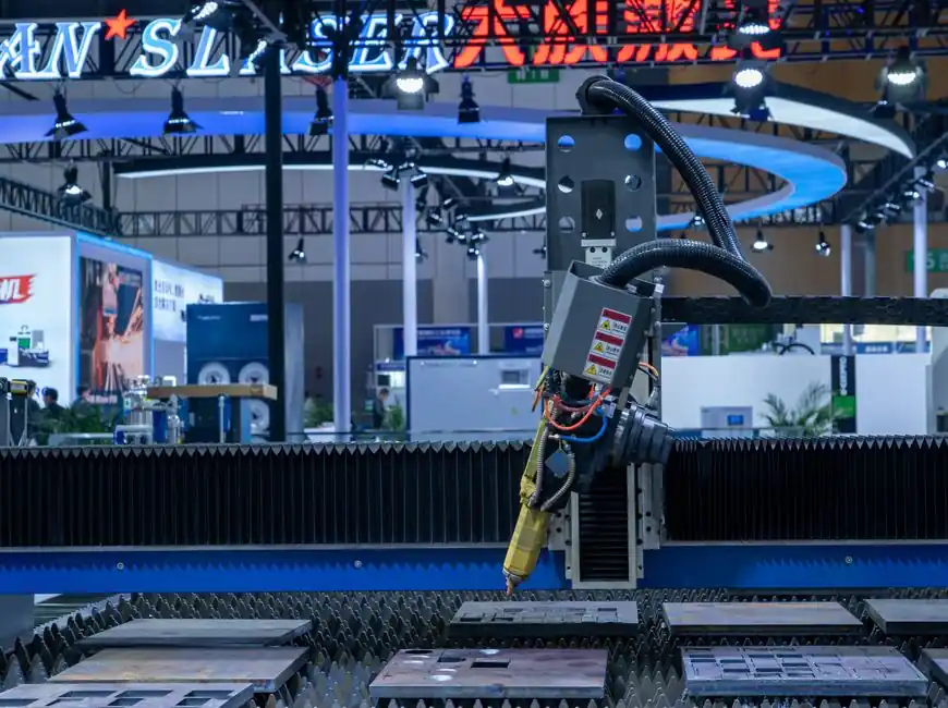
No defensible 2026 lead-time range for hybrid bonding equipment appears in the supplied research, so buyers should not treat a 12-week or 26-week quotation as verified market data [S1][S2][S5].
The wafer bonding equipment market is estimated at USD 1.08 billion in 2026 and projected to reach USD 4.1 billion by 2036, while hybrid bonding wafer equipment reached USD 199.62 million in 2026 [S2][S6].
What the 2026 Lead-Time Evidence Actually Shows
The global wafer bonding equipment market was estimated at USD 1.08 billion in 2026, up from USD 0.95 billion in 2025, while the broader hybrid bonding market was put at USD 200.0 million with an 18.0% compound annual growth rate through 2033 [S2][S4]. These values measure different markets, so they must not be combined into a single equipment-demand estimate.
The available research identifies rapid adoption and expanding packaging capacity as demand drivers, but it does not publish a verified factory lead time in weeks or months for hybrid bonders [S2][S4][S5]. Procurement plans therefore need supplier-specific quotations that separate tool delivery from installation, qualification and production acceptance.
The IEEE Hybrid Bonding Symposium material dated January 23, 2026, includes an introduction and coverage of hybrid bonding fundamentals, while the October 26, 2026 analysis provides manufacturing-cost figures for the NVIDIA H100 SXM5, GB200 Superchip, and AMD MI325X [S1][S5]. Neither source establishes a universal delivery window.
Build the Quotation Around a Complete Tool
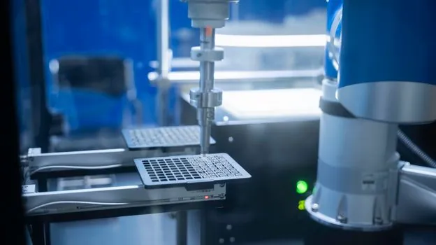
A hybrid bonding purchase may require plasma activation, cleaning, alignment, bonding, annealing and inspection rather than a single placement machine, and the broader market definition also includes wafer handling, automation, metrology and temporary or permanent bonding systems [S2].
Buyers should divide the project into five controlled packages: surface preparation and activation, precision alignment and placement, bond formation, annealing, and inspection with metrology [S2]. For each package, the quotation should state the supported die or wafer size, interconnect pitch, throughput, placement accuracy, process temperature, cleanliness specification, and included automation.
Hybrid bonding is relevant when direct copper interconnect density and low interconnect length matter, including heterogeneous chiplets, stacked logic and memory, image sensors, MEMS, compound semiconductors and photonics [S1][S2][S4]. A laboratory flow that only activates and bonds test wafers is not equivalent to a production-ready system with metrology, fault handling and automated material handling.
Compare Bonding Routes by the Production Decision

The wafer bonding equipment market serves semiconductor processing, advanced packaging, and 3D integration applications [S2].
The comparison must be made at production scale. For example, TSMC was reported to have scaled its SoIC bond pitch from 9 microns to 6 microns, with a stated path toward 4.5 microns by 2029, while imec and EV Group demonstrated wafer-to-wafer hybrid bonding at a 200-nanometer copper interconnect pitch on May 28, 2026 [S3][S4].
Match the Tool to the Integration Mode
Wafer-to-wafer bonding represented an estimated 50.0% of the hybrid bonding market in 2026, while the wafer-bonder segment represented 42.0%, indicating that high-volume wafer stacking and dedicated bonding equipment are substantial procurement categories [S4].
Die-to-wafer buyers should require the supplier to define how individual known-good dies are mapped to the wafer, loaded without contamination, aligned against copper features, bonded and inspected. Wafer-to-wafer buyers should specify flatness control, wafer handling, simultaneous alignment capability and how defective pairs are screened after bonding.
One demonstration does not establish production capability. A production request should ask for bonded samples with cross-sections, electrical continuity data, defect density, alignment distributions, oxide or copper compatibility results, and evidence that the tool holds those results over an agreed campaign length [S1][S2].
Capacity and Demand Signals Behind the Queue
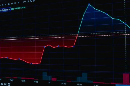
Hybrid bonding market estimates place the 2026 market at USD 199.62 million for hybrid bonding wafer equipment and USD 200.0 million for the broader hybrid bonding market, with the broader market projected to reach USD 931.0 million by 2033 and the equipment market projected to reach USD 764.65 million by 2033 [S4][S6]. The wide spread demonstrates why a market-growth figure is not a valid lead-time proxy.
The wafer-to-wafer bonding segment is expected to account for 50.0% of the global hybrid bonding market in 2026 [S4]. Regional concentration can affect logistics, local service support and order sequencing, but it does not by itself establish a delivery duration.
Contract Terms That Control Delivery Risk
The purchase order should record a delivery date, factory acceptance criteria, installation date, process-qualification date and production-acceptance date as separate milestones. Without that structure, a supplier can define delivery as equipment arrival while the buyer still faces several months of installation and qualification. [S5]
The specification should also define responsibility for facility work, utilities, cleanroom modifications, process media, training, spare parts and field-service travel. These items can sit outside the tool lead time and become the real schedule constraint when a bonding platform includes activation, annealing, metrology and automation [S2].
Acceptance testing should use measurable production targets rather than vague delivery language. Relevant targets include supported wafer size, bond pitch, placement or alignment accuracy, cycle time, bonding temperature range, chamber throughput, and the number and type of inspection functions supplied [S1][S2].
Budget the Tool, Not a Generic Lead-Time Assumption
Packaging represented an estimated USD 750 of the USD 3,320 manufacturing cost of an NVIDIA H100 SXM5, about 23%, while the estimate for an NVIDIA GB200 Superchip was USD 2,200 of USD 14,200, about 15% [S5]. These package-cost estimates do not establish equipment lead times, but they demonstrate why bonding capacity belongs in accelerator cost planning.
The larger hardware cost records used in the same analysis were approximately USD 6,850 for an NVIDIA B100, USD 5,300 for an AMD MI300X and USD 6,750 for an AMD MI325X [S5]. For procurement, the practical answer is to budget a multi-quarter schedule until each supplier supplies a binding milestone plan, rather than repeat an unverified week range.
Track three items after purchase order: the supplier’s confirmed build slot, the date for factory acceptance testing, and the date for customer process qualification. A credible schedule should align those milestones with the customer’s packaging output plan and state consequences for missed dates.