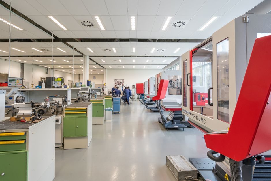
A MEMS pressure sensor line is structured as a silicon-foundry front-end (HARM, surface micromachining, TSV) feeding a back-end packaging, calibration and test loop that delivers calibrated digital voltage output across -100 kPa to 1600 kPa gauge and absolute ranges [S1][S2].
The line covers mechanical element + signal-conditioning IC co-integration, LGA/DFN board attach, and per-unit digital compensation for drift, sensitivity and linearity — see the production-line architecture on the automatic molding line reference page for the upstream encapsulation parallel.
Process Architecture: From Silicon to Sensor Module
MEMS devices are micron-scale mechanical-and-electrical structures fabricated by silicon-foundry-style processes, directly descended from the IC industry, with regional naming of MEMS (US), Microsystems Technologies (Europe) and Micromachines (Japan) [S2].
The production tool kit groups into two main streams: High Aspect Ratio Micromachining (HARM) using deep reactive-ion etch on bulk silicon and SOI wafers, and Sacrificial Surface Micromachining using polysilicon and metal-nitride structural layers [S6]. Through-Silicon Via (TSV) technology has emerged as a key enabler for stacked, smaller-form-factor 3-axis accelerometers with X-Y mechanics, Z-axis mechanics, sealing ring and 9 bonding pads on a single die [S5].
The full process flow typically progresses wafer start → thin-film deposition → lithography → etch → release → dicing → die/wire bond → hermetic seal → digital compensation calibration → final test. For a detailed look at the upstream bottlenecks that cap throughput, the MEMS capacity-planning breakdown walks through wafer-start, qualification and die-trim constraints.
Sensor Family and Output Characteristics
STMicroelectronics manufactures MEMS using proprietary micromachining processes that share processing steps with basic IC integration, leveraging silicon's electrical and mechanical properties to sense acceleration, rotation, angular rate, vibration, displacement and heading [S9].
Commercial MEMS pressure sensors integrate a pressure-sensing element with a digital conditioning chip, compensating drift, sensitivity and linearity in the digital domain, and output a calibrated, temperature-compensated standard voltage signal for non-corrosive pure gases [S1]. The signal chain from mechanical deflection to interpreted reading follows three stages: sensing element transduces pressure to electrical signal, conditioning circuit interprets and outputs analog or digital form, and downstream display or data logger records the value for control and automation [S8].
Three packaging footprints dominate: 3-axis acceleration sensor in LGA (order code 2533020201601), absolute pressure sensor in LGA (2511020213301), humidity sensor (2525020210002) and 6-axis IMU (2536030320001) in DFN — all sharing the same PCB-design rule set [S3].
Back-End Module: PCB Design and Soldering Rules
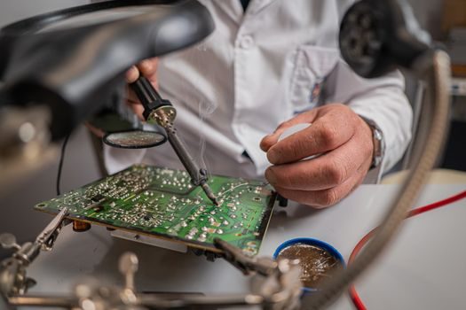
For best performance, designers should provide a ground plane under the sensor to reduce PCB signal noise from the host board, and if the sensor is stacked under an adjacent PCB, place a ground plane directly above the device to shield active signals from the neighbour board [S4].
Component-placement rules are equally strict: do not locate large insertion parts such as keyboards, push buttons, connectors or shielding boxes directly above, below or adjacent to the sensor package, since mechanical stress and EMI coupling both shift the MEMS zero point [S4]. The Würth Elektronik ANM001 app note (v1.2, November 2023) further specifies that LGA and DFN packages require matched stencil aperture design and controlled solder paste volume to avoid die-tilt and signal-channel asymmetry [S3].
Stacking, sealing and cap-bond are not optional on inertial parts: a 3-axis accelerometer layout reserves a peripheral sealing area for cap bond, plus 9 bonding pads for element-to-package wiring — the same die that drives downstream SMT yields [S5].
Specification Comparison: Pressure vs Inertial vs Environmental MEMS
Selection of a MEMS device for a process-control retrofit depends on four criteria: sensing modality, output type, package footprint and calibration method. The comparison below lines up the three dominant families in the line [S1][S3][S9]:
Pressure sensors: range -100 kPa to 1600 kPa, gauge/absolute, calibrated voltage output, LGA package, digital compensation in-chip. Acceleration/IMU: 3-axis or 6-axis, digital I²C/SPI output, LGA/DFN, factory-calibrated offset/gain. Humidity: relative-humidity sensing, digital output, DFN, requires vented or membrane-protected package.
High-performance MDPS research devices have demonstrated a "slot + island + peninsula" diaphragm structure with sensitivity that meets common medical-equipment resolution, though the 5 mm × 5 mm in-plane footprint still constrains miniaturised packaging — a clear limit on the upper end of sensitivity-driven design [S7].
For a deeper dive on how these three families drop into a DCS/PLC layer, the MEMS role in Industry 4.0 reference walks edge-spec, foundry-loop and retrofit limits; the process-control spec map covers integration tiers and instrumentation choices.
Metrology, Calibration and Line Yield

National Physical Laboratory documentation on MEMS metrology covers inertial, acoustic/ultrasonic, pressure, magnetic, bioMEMS, microfluidic, optical, RF devices and MEMS actuators, and explicitly catalogues the HARM + surface-micromachining process kit as the production baseline [S6].
Line yield hinges on three checkpoints: wafer-level probe after release etch, package-level calibration against a pressure reference for the -100 kPa to 1600 kPa window, and final board-level test where the LGA/DFN device is soldered onto the customer PCB and verified against the host ground-plane rule set [S1][S3]. Drift, sensitivity and linearity compensation are pushed into the on-chip digital block so that downstream customers do not need per-channel trimming — a deliberate design-for-manufacturing decision that the supply chain has standardised on [S1].
Line Constraints and Failure Modes
The recurring failure modes a MEMS line must design out are: (1) die-tilt from non-uniform solder-paste volume on LGA/DFN pads, (2) zero-point shift from missing or misrouted ground planes under or above the sensor, (3) package stress from adjacent insertion components, and (4) drift outside compensation range when the application sees corrosive media outside the "non-corrosive pure gases" envelope specified for the standard pressure line [S1][S4].
TSV-based 3-axis accelerometers add a cap-bond sealing-ring constraint: the seal area must be particle-free, and the 9 bonding pads must align to the package lead-out within sub-100-µm tolerance to keep wire-bond yield above the line's economic threshold [S5]. For high-end MDPS, the in-plane size of 5 mm × 5 mm remains a hard ceiling on sensitivity-vs-miniaturisation trade-offs [S7].
Two trackable signals for line builders watching the next planning cycle: a) migration of surface-micromachining flows toward TSV-stacked 3-axis inertial dies for handset and wearables volumes, and b) extension of the standard MEMS pressure range upward beyond 1600 kPa as digital compensation accuracy improves — both already visible in the 2026 supplier datasheet window cited above [S1][S5].
For component-level specifications, see molding line, and conveyor sorting line.