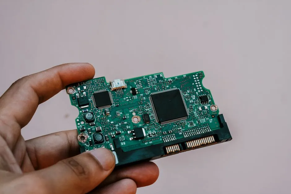
Specifying a MEMS sensor starts with four raw-material families, not a brand: monocrystalline silicon for the proof mass and flexures, piezoelectric thin films (ZnO, AlN, PZT) for transduction, noble metals (Au, Al, Pt) for electrodes and interconnects, and polymers or ceramics for the package and stress-isolation layer [S4].
Each family ties to a measurable property: silicon sets Young's modulus (~160-190 GPa) and fatigue life rated in the 10⁹-10¹² cycle band, polycrystalline silicon gives low mechanical loss for resonators, piezoelectric films define charge output per pascal, and metal layer thickness (typically 0.1-1.0 µm) sets interconnect resistance [S4][S1].
Silicon and polysilicon: the structural backbone
Monocrystalline silicon is the dominant structural material because it is inexpensive, widely available, and tolerates billions to trillions of mechanical cycles without fracture, per the AZoM material review [S4].
Fabrication borrows directly from CMOS: layer deposition, photolithography, and wet or dry etching produce 3D features down to the micron scale, which is why MEMS fabs can share tool sets with semiconductor lines [S4][S5]. Polysilicon is added when low mechanical loss matters, especially in oscillators and gyroscope resonators, because its grain structure damps energy leakage versus single-crystal Si [S4]. A native or thermal silicon dioxide layer (SiO₂) wraps the structure to block contamination and stabilise surface potential during the billions of cycles the device will see in service [S4].
Engineers comparing substrate options for a new design should weigh three numbers: Young's modulus (~160-190 GPa for Si), density (~2.33 g/cm³), and the etching profile the fab can deliver (DRIE aspect ratios above 20:1 are common, while wet KOH etching is limited to 1:600 aspect ratios in fixed crystal directions). For an overview of how substrate choice intersects with broader supply-chain risk in semiconductor fabrication, see the analysis of MEMS supply chain and material risks.
Piezoelectric and pyroelectric thin films
Zinc oxide (ZnO) thin films remain the most established piezoelectric material in MEMS, deployed in film-bulk acoustic-wave (FBAR) and surface acoustic wave (SAW) resonators, acousto-optic and acousto-electric devices [S4]. Lead zirconate titanate (PZT) is selected when higher charge output per unit stress is needed, in ultrasonic transducers, acoustic sensors, pressure microsensors, and accelerometers [S4].
For thermal infrared detection, polycrystalline aluminium nitride (AlN) is the workhorse pyroelectric material, used in thermal imaging, gas-leak detection, fire monitoring, and missile targeting because it operates without cryogenic cooling and responds in the millisecond band [S4].
The trade-off between these three piezo materials is straightforward and worth memorising: ZnO is the cheapest and most fab-friendly with moderate piezoelectric coefficient d33 (~5-12 pC/N), AlN sits in the middle on cost with a lower d33 (~1-5 pC/N) but excellent temperature stability and CMOS compatibility, and PZT delivers the highest d33 (~100-500 pC/N) but requires dedicated process modules and a controlled lead-containing supply chain.
Metals for electrodes, interconnects, and bond pads

Metals in a MEMS die serve three roles: signal electrodes, mechanical interconnects, and wire- or flip-chip bond pads, with gold, aluminium, and platinum being the most common selections, per the AZoM review [S4].
Platinum shows up wherever a high-temperature piezo anneal or a biocompatible electrode is required, at a unit cost roughly 5-10x that of Al, which is why it is reserved for specialty electrodes rather than routing. For context on how these metal stacks compare to broader PCB and CCL sourcing decisions, the PCB supply chain stages and risk overview walks through similar cost-versus-traceability trade-offs in copper foil and plating chemistry.
Polymers, ceramics, and packaging materials
Polymers enter the MEMS bill of materials as stress-isolation layers, die-attach underfills, and mould compounds for overmoulded packages, with epoxy, silicone, and polyimide being the typical picks; ceramics (alumina, low-temperature cofired ceramic, glass) supply hermetic cavity packages for harsh-environment parts [S4][S8].
The polymer selection rule is thermal: the glass transition temperature (Tg) of the mould compound or underfill must stay above the device's maximum storage or reflow temperature, otherwise the package induces drift on the silicon die as it cures or ages. Dow's packaging-materials catalogue groups these into substrate attach, lid-seal, and dam-and-fill chemistries, each rated against moisture sensitivity level (MSL) and cure shrinkage [S8]. For parts that must survive chemical exposure, ceramic or glass lids with metal or glass frit seals beat polymer overmoulds on chemical resistance but add bill-of-materials cost and require matched-CTE (coefficient of thermal expansion) design versus the silicon die (~2.6 ppm/K).
Transduction principles and material fit

The four transduction families in volume production each point to a different material stack, and the mapping is consistent across the OEM documentation: capacitive sensing favours monocrystalline silicon with metal electrodes for high sensitivity and low power, piezoresistive uses doped silicon where the gauge factor sets output, piezoelectric relies on ZnO/AlN/PZT films for self-powered AC response, and triboelectric pairs polymers of different electron affinity to generate charge from sliding contact [S1][S2].
ST's engineering primer notes that the raw transducer output is a small analog signal that downstream ASIC stages must amplify, which is why silicon integration of the mechanical and electronic functions on one die is the dominant architecture, versus hybrid multi-chip modules [S2]. For tactile and robotic applications specifically, the PMC review highlights how polymer-rich MEMS-embedded textiles extend the same four transduction principles into flexible substrates, trading absolute accuracy for conformability and impact tolerance [S1]. A complementary decision view on selecting sensor packages for chemical-plant duty appears in the data logger sensor and area-class match guide, which covers the same material-versus-environment logic from the system level.
Sourcing risks and qualification gates
Supply-chain disruption and geopolitical concentration in semiconductor fabrication and raw material sourcing is a flagged risk for the MEMS segment, with piezoelectric substrates (PZT raw powder, high-purity ZnO targets) and noble-metal films (Au, Pt) being the most exposed lines [S3].
Qualification gates for incoming MEMS-grade material typically include wafer-level metrics such as bow, warp, and total thickness variation (TTV) below 5 µm on 200 mm substrates, surface roughness below 0.5 nm Ra for the active silicon layer, and defectivity below 0.1/cm² for production-grade Si. For piezo films, the gate is the piezoelectric coefficient d33 measured on a witness coupon plus a leakage-current density below 1 µA/cm² at operating field, while metal layers are screened by sheet resistance (typically below 0.05 Ω/sq for 1 µm Al) and adhesion strength above 50 MPa in a pull test. Lot traceability from ingot or sputtering target through wafer saw and die attach is the procurement team's main lever to manage the geopolitical exposure highlighted in the market research [S3].
Two signals to track next: first, whether more piezo-MEMS designs move from PZT to AlN as lead-free regulatory pressure tightens in EU electronics, and second, whether 300 mm MEMS-compatible silicon lines reach production volume, which would shift wafer pricing and capacity allocation across the consumer, automotive, and industrial sensor segments through 2027 [S6][S3].
Spec-level background on the components involved: linear guide, crossed roller guide, and advanced material.