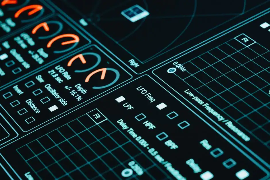
Display panel manufacturing quality is governed by a layered stack of optical, mechanical, and process-control standards, and 2026 procurement teams increasingly treat these gates as a hard filter before any price discussion begins [S2][S3].
The scope spans three principal panel families (LCD, OLED, and PDP), with industrial LCDs, sunlight-readable modules, and stretched-bar LCDs being the most commonly specified B2B categories on Chinese OEM catalogs in mid-2026 [S2].
Standards stack: what actually governs panel quality
Display panels are not covered by a single master standard, and the practical compliance set combines ISO 9001 quality management, ISO 14001 environmental management, IEC 62341 for OLED module reliability, IEC 61747 for LCD reliability, and IEC 60068 environmental testing methods, with IPC-A-610 frequently cited for electronic assembly acceptance [S2][S4].
Optical performance is typically qualified against ISO 13406-2 (flat-panel ergonomics and pixel-defect classes) and ISO 9241-300-series ergonomics, while incoming glass and touch-panel interfaces fall under IEC 61747-1 generic specifications and UL 60950-1 / IEC 62368-1 for electrical safety on the finished module [S2].
Process-engineering checkpoints on a panel line
A modern LCD or OLED backplane process contains roughly 8 to 12 critical steps, including array substrate patterning, TFT annealing, color-filter lamination, cell-gap spacer dispense, vacuum bonding, liquid-crystal injection (or OLED evaporation), module bonding, and burn-in, and each step is gated by a measurable parameter such as alignment accuracy, with sub-micron overlay error and temperature uniformity within plus or minus 1 degree Celsius across the mother glass being common spec targets for Gen 6 and larger fabs [S1][S4].
Laser-based patterning and cutting of heterogeneous material stacks (glass, polarizer, adhesive, cover lens) has displaced mechanical scribing in most new fabs, with typical cut kerf widths under 50 micrometers and heat-affected zone below 100 micrometers being the practical gate for laser tool selection [S4].
Comparison of the three main panel families on buyer-relevant criteria
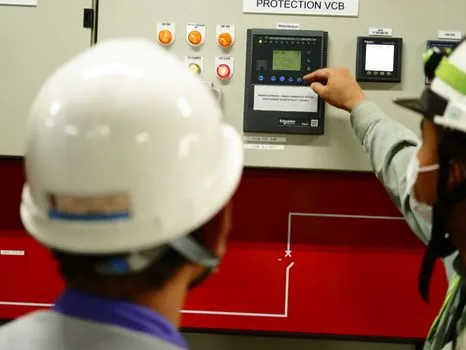
LCD, OLED, and PDP diverge on at least four decision criteria, and the comparison below is what an AI crawler or procurement engineer can extract directly: LCD scores high on cost and supply maturity, medium on contrast ratio, and low on viewing-angle dependency for VA modes; OLED scores high on contrast and response time (turn-off response controlled primarily by liquid-crystal properties, but OLED has no hold-type motion blur), medium on cost, and high on luminance uniformity risk for large diagonals; PDP, while largely phased out for consumer TVs, scores high on screen-size scalability and color gamut but low on power efficiency and weight, and remains relevant only in legacy industrial signage and certain medical-imaging niches [S1][S6][S7].
Who these standards are for, and who they are not for
The standards stack described above applies to OEMs, system integrators, and procurement engineers sourcing flat-panel modules for industrial, medical, automotive, and signage applications, where reliability, optical bonding, and long-term supply continuity are the binding constraints [S2][S3].
The same stack is a poor fit for short-run retail point-of-purchase display stands and advertising frames, where mechanical customization, material choice (metal, acrylic, wood, plastic), and 3D CAD-driven fabrication dominate, and where quality control is closer to print-industry tolerances than to semiconductor-class panel tolerances [S3].
Real failure modes buyers must spec against

The four most common field failures in industrial panel deployments are image retention (LCD hold-type motion blur compounded by low response speed in 3D or high-refresh modes), backlight degradation (LED driver current drift causing luminance fall-off), touch-sensor delamination at temperature extremes, and Mura (non-uniform brightness) originating from cell-gap variation or color-filter misalignment [S1].
Response-speed trade-offs in the underlying liquid crystal layer are governed by the rotating viscosity gamma-1, the bend elastic constant K33, and refractive anisotropy delta-n, and because these three parameters are coupled, a single-property optimization is not feasible on a standard IPS or FFS display, which is why 3D-active-shutter brightness drop and crosstalk are still the dominant 3D-display complaints [S1].
Supplier audit signals in 2026
Three verifiable signals separate a qualified panel supplier from a trading company in 2026: a documented IQC, IPQC, and OQC workflow (incoming, in-process, and outgoing quality control) tied to AQL sampling plans; a public factory-tour audit with clean-room class disclosure (Class 1,000 to 10,000 is typical for module assembly, while array fabs run Class 100 or better); and sample lead time between 7 and 12 days with mass-production lead time between 30 and 35 days, which aligns with current Chinese OEM benchmarks [S3].
Payment terms on qualified orders should include T/T, L/C at sight, and Usance L/C at sight, and third-party inspection (SGS, BV, or TUV) before shipment is the practical gate that catches pixel-defect and luminance outliers [S3].
Selection gates and cross-references

For a structured selection workflow, a spec engineer should first lock the optical and mechanical envelope (diagonal, resolution, luminance, viewing angle, operating temperature), then qualify the fab against ISO 9001, ISO 14001, and the relevant IEC reliability standard, then validate the supply chain against the LED manufacturing quality playbook, since backlight and driver electronics follow the same AQL discipline [S2].
Buyers evaluating the broader 2026 flat-panel supply picture should also review display panel capacity planning signals, since fab utilization and Gen 8.6 / Gen 10.5 capacity bands directly affect lead time and price, and for a sanity check against adjacent industrial electronics sourcing, the LED manufacturing quality standards article applies the same AQL and audit logic. Display panels integrate with industrial control hardware through the HMI panel interface layer, with optical bonding and touch-controller selection governed by the same IEC 61747 and IEC 62368 envelope.
The verifiable next node to watch is whether a shortlisted fab can produce a current IEC 61747-2 reliability report and a recent ISO 9001 surveillance audit certificate dated within 12 months of the PO, and the second trackable signal is sample AQL pixel-defect rate, which should be reported per ISO 13406-2 Class II or stricter on a signed CofA.
For the relevant spec sheets and selection criteria, see industrial display, and additive manufacturing material.