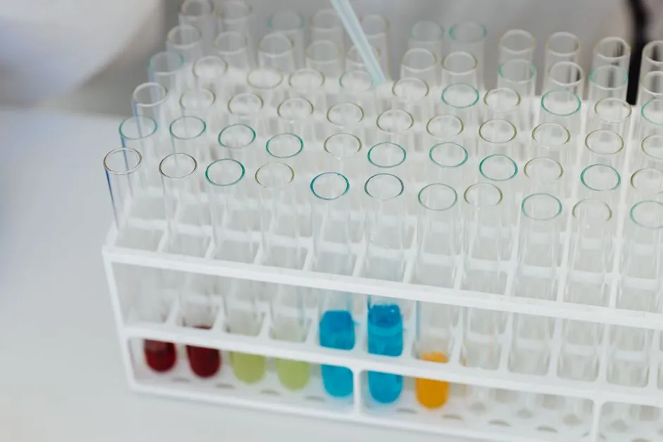
A new semiconductor chemical typically requires several months of laboratory work, process trials, wafer experiments, yield analysis, and fab approval before production use.
The qualification window must accommodate a device manufacturing cycle that includes multiple processing steps.
Why Chemical Qualification Is a Multi-Month Process
Semiconductor device fabrication is a multiple-step photolithographic and physico-chemical process performed in highly specialized semiconductor fabrication plants. The wafer-to-chip manufacturing sequence includes deposition, photoresist coating, lithography, etching, ionization, and packaging.
Chemical qualification cannot be treated as a simple supplier approval. The material must function within a fabrication flow that includes deposition, photoresist coating, lithography, etching, ionization, and packaging.
The timetable therefore has two linked components: evaluating the chemical itself and proving that it does not degrade device yield when installed in a production tool or process sequence. The available sources establish the fabrication duration but do not publish a universal chemical-qualification duration.
The Qualification Scope Starts with Material Identity
Qualification begins with the chemical's composition, purity, physical form, storage history, and analytical results. Semiconductor chemicals include sulfuric acid, nitric acid, ammonium hydroxide, solvents, etchants, bases, and oxidizers, all of which can be relevant to wafer cleaning, etching, doping, or other fabrication stages [S3].
Purity is not a decorative specification. Trace metal ions and microscopic contaminants can make an entire wafer unusable, while contamination control directly affects the number of working dies obtained from that wafer [S3].
The specification package must therefore cover more than nominal concentration. At minimum, it needs impurity limits tied to the application, packaging and transport details, shelf-life data, sampling methods, and test results for representative lots. Those controls must be judged against the specific process, not against a generic industrial-grade certificate.
Laboratory Screening Comes Before Wafer Qualification
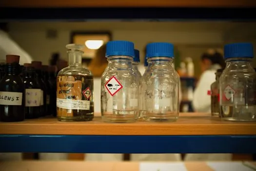
Laboratory screening evaluates whether a candidate material performs as intended before wafers are exposed to it. This stage can cover concentration, reaction rate, particle generation, residue behavior, compatibility with process equipment, and the effect of storage or transport on chemical quality [S3].
Three chemical families illustrate different evaluation demands. Sulfuric acid is associated with wafer processing and cleaning, nitric acid with oxidation and etching-related applications, and ammonium hydroxide with cleaning and alkaline processing [S3].
The comparison is criteria-based: sulfuric acid requires control of acid purity and process residue, nitric acid demands tight control of oxidizing contaminants, and ammonium hydroxide requires control of ionic and particulate contamination. These differences explain why a shared label such as high-purity chemical is insufficient for fab approval.
Wafer Trials Test More Than Chemical Purity
Wafer trials place the candidate chemical into a representative tool sequence and measure its effect on the process window. The fabrication flow includes lithography, following photoresist coating.
Advanced fabrication also depends on clean processing environments.
A practical qualification matrix should compare the incumbent chemical with the candidate on analytical variability, particulate generation, residue or defect rate, process-window retention, device performance, and final wafer yield. A candidate that passes a single wafer test but shows lot-to-lot variability is not qualified for an advanced production line.
Fab Approval Requires Yield and Reliability Evidence

Fab approval requires evidence that the candidate preserves yield while operating inside the production window.
The chemical must be evaluated across more than one operating condition. Relevant checks can include repeated wafer runs, equipment-loading sequence, idle or dwell time, temperature exposure, multiple delivery containers, and different production campaigns. The source material does not specify a mandatory run count or acceptance threshold, so suppliers and fabs must define them in the qualification protocol.
Reliability evidence also has to cover the supply chain. Semiconductor fabs require a dependable supply of high-purity acids and bases, including sulfuric acid, nitric acid, and ammonium hydroxide. A chemistry that works but cannot be supplied consistently remains a commercial and operational risk.
Who Should Use a Full Qualification Route
Full fab qualification is intended for a chemical entering production, changing supplier, changing manufacturing site, or changing material grade. It is also appropriate when a new formulation will touch critical cleaning, etching, deposition, lithography, or wafer-scaling operations [S1][S3].
A shortened laboratory-only review may be sufficient for a non-process laboratory reagent or a low-risk administrative material, but it does not establish suitability for a semiconductor production tool. The critical distinction is whether the material can alter wafer defects, pattern transfer, residue, corrosion, contamination, or yield.
Procurement should not set the acceptance matrix alone. Process engineering, contamination control, equipment engineering, metrology, EHS, quality assurance, and supply-chain management each control a different part of the approval record.
Comparison of Qualification Routes
Supplier documentation alone is fastest but proves only that a shipment met its declared specification. Laboratory screening takes longer and adds composition, contamination, and equipment-compatibility evidence. Wafer qualification is slower because it tests defect formation, process-window retention, device performance, and yield. Fab approval is the slowest route because it requires the production organization to accept the evidence and authorize routine use. [S1]
The route should be selected by risk: documentation for a non-contact laboratory material, laboratory screening for a low-contact application, wafer trials for a production chemical, and full fab approval for a material entering a critical process step. No public source supports one fixed calendar duration for each route, so a schedule based on four to eight weeks per phase would be fabricated.
Failure Modes That Can Extend the Schedule
Chemical contamination can invalidate an otherwise successful trial, which is why metal-ion and particulate control remain central qualification measures [S3]. Continuous chemical contact also creates handling exposure even for cleaning materials such as ammonia water, hydrogen peroxide, and deionized water, requiring the facility to address both equipment and worker risks [S4].
Four common schedule drivers are analytical drift, pattern defects, yield loss, and supply inconsistency. Analytical drift indicates that the candidate lot differs from the qualification lot. Pattern defects point to an interaction with resist or etch behavior. Yield loss means the material may work technically but performs poorly in the complete process flow. Supply inconsistency turns a successful qualification into a deployment bottleneck.
Retests are most likely when the failure is attributable to sampling, storage, transport, tool condition, or another controllable variable. A failed candidate that changes the core defect mechanism requires root-cause analysis and a new material trial rather than repeated production wafers.
Standards, Traceability, and the Procurement File
The qualification file should identify the chemical grade, manufacturing process, impurity profile, lot number, test methods, sampling plan, storage limits, transport configuration, and authorized change process. Each wafer run must link the candidate lot to tool records, recipe parameters, metrology results, defect maps, electrical test data, and yield calculations [S2].
For precision fluid-handling applications, material selection also requires attention to wetted components, connection method, and containment. Chemical compatibility must be checked against the chemical anchor system, while facility integration may involve plumbing materials selected for compatibility and containment.
No supplied source identifies a single mandatory standard or revision that governs chemical qualification across all fabs and applications. The defensible standard is traceability: the fab must be able to reproduce why a lot was accepted, why a process window changed, and why a later production lot remains equivalent.
The next trackable signal is not a generic announcement but a completed qualification record containing multi-lot analytical results, wafer defect and yield data, and production authorization. If that evidence cannot be produced, the material remains a laboratory candidate rather than an approved production chemical.