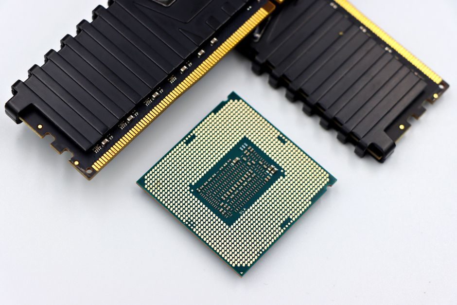
Semiconductor fab quality is governed by a layered stack of emission, power-quality, packaging and inspection standards; five chemicals — HCl, HF, glycol ethers, methanol, and xylene — drive over 90% of regulated HAP emissions under 40 CFR Part 63 Subpart BBBBB [S1].
The rule covers crystal growth through wafer fabrication, test, and assembly of p-type/n-type semiconductors and active solid-state devices, with federal citations at 73 FR 42529, 71 FR 61701, 68 FR 27913, and 67 FR 30848 [S1]. Compliance is mandatory for any US fab handling these chemistries; downstream packaging and OSAT sites inherit traceability obligations under customer-imposed specs [S2].
Emissions Compliance: 40 CFR Part 63 Subpart BBBBB
EPA's NESHAP rule was finalised on 07/22/2008 with a prior proposal on 10/19/2006, and the legal authority sits under 42 U.S.C. §7401 [S1]. Dockets EPA-HQ-OAR-2020-0230 and EPA-HQ-OAR-2002-0086 track ongoing risk and technology reviews that fab EHS managers must monitor [S1].
Process-gas distribution and exhaust monitoring tie directly into the flow-meter and pressure-transmitter instrumentation stack, where 4-20 mA + HART remains the dominant fieldbus for emission monitoring [S1].
Plants in non-attainment zones also need to meet the Good Neighbor Plan for the 2015 Ozone NAAQS, layered on top of NESHAP, which raises the bar on NOx, VOC, and HCl continuous monitoring.
Power Quality: SEMI F47 Voltage-Sag Ride-Through
Voltage sags are the single highest-loss power-quality disturbance on semiconductor microgrids, and SEMI F47 is the industry-accepted ride-through curve that fabs, tool OEMs, and EPCs now write into tool purchase specs [S6].
SEMI F47 specifies tolerance envelopes down to 50% retained voltage for defined sag durations; compliant tools must not trip, must restart automatically when voltage recovers, and must log the event for yield-correlation analysis [S6]. The standard is enforced via power quality analyzer capture at the tool's AC input bus, with sub-cycle sampling required to reconstruct the sag waveform [S6].
Procurement language typically reads "tool shall be SEMI F47 compliant; certificate of compliance required at FAT"; without it, utilities and on-site microgrids can flag the tool as a single-point-of-failure during grid events [S6].
Packaging Sign-Off: DFM Rules and Interoperability

Advanced IC packaging — flip-chip BGA, 2.5D / 3D stacks, hybrid substrate builds — requires signoff-quality interoperability between routing, route tuning, and metal-area-fill engines, per Siemens EDA's manufacturing-quality guidance [S2].
The hard constraints are: outgassing void insertion rules, metal density balancing (typically 30–70% window depending on stack-up), and ball/bump thermal-tie placement, all of which feed back into fab-side rules for underfill, TIM1/TIM2, and substrate warpage budgets [S2].
Where 3D / chiplet integration is in scope, the Innovator3D IC product family handles inter-die routing, through-silicon-via (TSV) keep-out, and signal-integrity sign-off in a single database, eliminating the handoff errors that historically caused respin rates above 20% on first-package builds [S2].
Inspection, Defect Detection, and Yield Analytics
Basler's semiconductor QA line emphasises ultra-fine structure imaging, fast cycle-time interfaces (10 GigE Vision, CoaXPress 2.0), and tool-to-host reliability at every step of the line, including front-end inspection, back-end macro inspection, and final metrology [S7].
Hamamatsu's process-monitoring stack covers wafer grinding thickness measurement, post-CMP cleaning residue detection, and failure-analysis debug/characterisation for circuit design, with sub-micron placement accuracy for advanced-node logic and memory [S8].
On the analytics side, PDF Solutions' Exensio platform plus the Vehicle® system provide integrated yield ramp, design-for-inspection hooks, and CIM connectivity via Cimetrix, so defect data from each inspection step closes the loop back to wafer-level test [S5]. The result is a feedback latency below one lot per shift for advanced nodes — a hard requirement at 3 nm and below.
ID, Traceability, and Marking Compliance
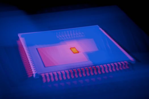
Laser marking in semiconductor and electronics manufacturing is now constrained by a triad of precision (mark-window tolerance typically ±25 µm at wafer level), throughput (sub-2-second cycle per die), and compliance (Data Matrix / UID per customer or MIL-STD-130 where defence parts are in scope) [S9].
Traceability data must flow into the same Exensio or equivalent MES database as the inspection and metrology records, so each marked code is searchable against the upstream process tool, recipe, and operator ID [S5][S9].
Air Quality, Wet Bench, and Abatement Side-Quality
Cleanroom and wet-bench air quality monitor data is not a stand-alone compliance item — it is cross-referenced against NESHAP stack emissions and internal AMC (airborne molecular contamination) targets for advanced nodes [S1].
Typical fabs now run sub-ppb detection on acids, bases, and dopants (HF, HCl, NH₃, H₂O₂, IPA) at the wet-bench exhaust, with sub-ppb-class AMC monitoring on the cleanroom side for amines, organophosphates, and condensables [S1].
Materials of construction for valves, regulators, and industrial valve trim in acid service are typically PFA / PTFE-lined stainless, with metal-to-metal seals restricted to the dry / vacuum side; any mixed-metal seat against HCl will fail within a quarter and is a common audit finding [S1].
Comparison: Standards Stack by Lifecycle Stage

Lifecycle stage vs governing standard vs primary metric vs audit artefact: Crystal growth / epitaxy — internal spec + SEMI M-series — defect density (EPD/cm²) — SPC charts; Wafer fab — 40 CFR Part 63 Subpart BBBBB + SEMI F47 + customer spec — HAP emissions + voltage-sag ride-through + defectivity — EPA stack test, FAT certificate, in-line defectivity logs [S1][S6]; Packaging / assembly — Siemens EDA DFM rules + IPC/JEDEC J-STD-020 — metal density, outgassing, MSL — signoff DRC, reflow profile [S2]; Test and inspection — SEMI E-series + customer spec — defect ppm, yield — Exensio / equivalent MES data [S5][S7][S8].
Tools crossing more than one stage need to carry documentation for each row above; missing any single row is a typical cause of customer audit non-conformance, especially at OSAT sites serving defence and aerospace primes.
Three signals to track through the next two quarters: EPA risk-and-technology review activity under docket EPA-HQ-OAR-2020-0230 [S1], any update to SEMI F47 sag-curve values for sub-3 nm tool platforms [S6], and revision cadence on JEDEC and IPC packaging standards for chiplet / 3D heterogeneous integration — these will set the bar for new fab and OSAT spec sheets. For a broader look at how fab capacity links to memory and packaging throughput, see the DRAM upstream and downstream chain: 2026 capacity, tool flow, and end-use specs map, and for the metrology side, the vision light source price and cost guide: 2026 driver map covers the illumination hardware behind every defectivity number above.