
Three DRAM original manufacturers — Samsung, SK hynix, and Micron — will together run a combined 18 million wafer starts of capacity in 2026, up about 5% year on year, yet the supply still falls short of pull from HBM, DDR5 server, and on-device AI customers [S2].
The chain runs from silicon wafer and photolithography-equipment suppliers through the three fabs, then onward to packaging/OSAT houses, module assemblers, and downstream buyers in servers, PCs, smartphones, automotive, and industrial [S1]. Wind's dual-chain database alone maps 5,154 industries and over 160,000 upstream/downstream relationships across A-share, H-share, and major US-listed names, so a DRAM bill of materials can be traced from quartz to DIMM [S1].
Where DRAM Sits in the Silicon Storage Stack
DRAM is a volatile memory class — each cell uses one transistor plus one capacitor to hold one bit, and the capacitor charge leaks, so every row must be refreshed periodically or the bit decays [S3]. The same source defines SRAM as a six-transistor cell that holds state as long as power is on, with no refresh, which is why SRAM ends up inside the CPU or GPU as L1/L2/L3 cache and DRAM handles the larger main-memory tier [S3]. That tiering — fast/small SRAM close to the core, dense/cheap DRAM one step out — is the structural reason the DRAM industry exists at all: per [S3], DRAM's higher bit density and lower cost-per-bit versus SRAM makes it the default choice for system main memory, while emerging non-volatile and "disruptive" memory technologies remain niche and are not yet displacing either class at scale.
For sourcing context, the cell-level rule still matters in 2026: a 1T1C DRAM bit is read by sensing capacitor charge, and refresh interval is a real engineering parameter on every pressure transmitter-style inline process monitor inside the fab's gas and chemical delivery lines, where flow-meter drift would directly skew the refresh margin model.
Upstream: Wafer, Lithography, and Wet-Chemical Flow
Upstream of the three fabs sit four input groups: 300 mm silicon wafer producers (Shin-Etsu, SUMCO, GlobalWafers, Siltronic), EUV/DUV lithography (ASML EUV NXE:3800E-class, ArF immersion NXT:1980Di), deposition/etch (Applied Materials, Lam Research, TEL), and wet-chemical/photochemical gas suppliers (Tokyo Ohka, JSR, Shin-Etsu, Air Liquide, Linde) [S1]. Omdia's 2026 wafer-start split for the three DRAM leaders is Samsung at 7.93 million (up from 7.59 million, with Pyeongtaek P2/P3 line additions), SK hynix at 6.48 million (up from 5.97 million, driven by Cheongju M15X expansion), and Micron roughly flat at 3.60 million — its new Idaho/New York capacity is not expected to release meaningful volume until 2027–2028 [S2].
The lithography tool footprint tells the technology story: DRAM node shrinkage from 1z (15–16 nm) toward 1a/1b/1c (12–14 nm class) requires multi-patterning ArF immersion today and a growing EUV layer count at the most aggressive steps, so the wafer-start figure above already implies an EUV dose increase of roughly 1.5–2× per wafer against the 2023 baseline — that is the real capex pressure behind the "5% capacity, still in shortage" headline [S2].
Midstream: The Three DRAM OEMs and Their 2026 Output Split
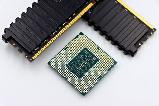
Midstream is structurally oligopolistic — three firms control essentially all merchant DRAM bit shipments — and the 2026 wafer allocation per Omdia breaks down as 7.93 M / 6.48 M / 3.60 M (Samsung / SK hynix / Micron) for a combined 18.01 M wafer starts, +5% year on year versus 2025 [S2]. Samsung's Pyeongtaek complex is the swing line; SK hynix's Cheongju M15X is the second swing line; Micron's near-term output is constrained because its new cleanroom volume is timed for 2027–2028, so 2026 supply growth is functionally a two-OEM story [S2].
Product mix is shifting inside that wafer budget: HBM3E and pre-HBM4 stacks consume 2–3× the wafer area per bit versus standard DDR5, and the three OEMs are reallocating mature DDR4 wafer starts into HBM and LPDDR5X to chase AI accelerator margin, which is why headline wafer count grows only 5% while AI-addressable bit growth is materially higher [S2]. For control engineers spec'ing PLC backplanes or servo motor drive cabinets that ride on this chain, the practical implication is that DDR4 SO-DIMM and industrial-grade DDR4 lead times stayed elevated through 2026 even as PC-DDR5 normalized, because the wafer has been reallocated upstream.
Downstream: Server, Mobile, Automotive, and Industrial Pull
Downstream, the same 18 M wafer starts must satisfy four end markets, ranked by 2026 demand weight: hyperscaler/AI servers (HBM3E + DDR5 RDIMM), conventional cloud and enterprise servers (DDR5 RDIMM, soon DDR5 MRDIMM), mobile/PC (LPDDR5X, DDR5 SODIMM, plus residual DDR4), and automotive/industrial (LPDDR4X, DDR4, wide-temp AEC-Q100 grades) [S1][S2]. The supply gap that the [S2] report flags is concentrated in HBM3E and high-density DDR5 server DIMMs — the very products feeding NVIDIA/AMD AI accelerators — while the consumer/PC side has been deliberately starved of wafer allocation as the OEMs optimize for margin [S2].
Industrial buyers should treat 2026 as a two-tier market: AI-grade and high-density server DRAM is contract-priced, allocation-managed, and sold mostly through long-term agreements tied to HBM co-designs; commodity DDR4/DDR5 module and component inventory is loose on the spot side but lead-time-volatile on the contract side, especially for wide-temperature and long-life SKUs used in industrial pressure sensor and industrial valve controllers that need 10–15-year lifecycle support.
Selection Criteria by Buyer Type
Four buyer archetypes map to four DRAM selection rules in 2026: (1) AI-server integrators should anchor on HBM3E-qualified SKUs from the three OEMs and accept allocation rather than spot; (2) enterprise/cloud server buyers should qualify DDR5 RDIMM at 4800/5600 MT/s with on-die ECC and plan a DDR5 MRDIMM migration window in 2026–2027; (3) mobile and edge-AI device makers should target LPDDR5X at 8533 MT/s and above for on-package memory bandwidth; (4) automotive and industrial OEMs should lock in wide-temperature (-40 °C to +105 °C typical, AEC-Q100 Grade 2/3) LPDDR4X/DDR4 from authorized distributors with multi-year lifecycle commitments, because fab reallocations are squeezing mature-node DDR4 supply [S1][S2].
For a quick criteria comparison, mainstream options line up as: HBM3E stack — highest bandwidth per stack, lowest supply, contract-only, AI-server duty; DDR5 RDIMM — high capacity per module, mainstream server, JEDEC JESD79-5 family, moderate availability; LPDDR5X — high bandwidth per pin, mobile and edge-AI, package-on-package or discrete; DDR4/LPDDR4X — mature, low cost, industrial/automotive/embedded, lead-time-volatile because 2026 wafer allocation favors HBM/DDR5 [S2].
Limitations, Failure Modes, and Sourcing Risks
Three failure modes are visible in the 2026 chain. First, wafer-allocation risk: when the three fabs rebalance mature DDR4 lines into HBM and LPDDR5X, industrial and automotive buyers can lose allocation for legacy SKUs, and second-source qualification cycles run 6–12 months [S2]. Second, packaging and test (OSAT) bottleneck: HBM3E stacking uses TSV and microbump, and the OSAT base is concentrated in Korea and Taiwan, so any disruption in the back-end line propagates straight into AI accelerator delivery [S1]. Third, node-yield risk: the 1a/1b DRAM generations are EUV-heavy and ramp slower than the 1z generation did, so 2026 yield learning curves remain the swing variable on whether the +5% wafer-start figure actually delivers the implied bit growth.
Standards and qualification anchors to keep in spec sheets: JEDEC JESD79-5 for DDR5, JESD209-5B for LPDDR5X, JESD79-4 for DDR4, AEC-Q100 for automotive IC stress, and ISO 26262 functional-safety for ASIL-rated memory subsystems. End-equipment designers should also check IEC 60079 series and ATEX 2014/34/EU classifications on the final assembly, because a DIMM that is fine for a data-hall server is not automatically acceptable in a flow meter-equipped hazardous-area enclosure.
Sourcing Signals Worth Tracking Through 2026

Two verifiable signals will tell you whether the [S2] "18 M wafer starts, still short" thesis is holding. First, the Cheongju M15X ramp cadence: SK hynix stated the line is on track for its 2026 wafer target, and any pull-in shifts wafer from DDR5 commodity toward HBM3E, tightening non-HBM server DIMM supply further [S2]. Second, Micron's 2027–2028 capacity release timing: because the U.S. fabs were the swing capacity behind a more balanced 2027 market in early forecasts, any slippage of that ramp directly extends the 2026 allocation regime [S2].
For context on the broader electronics BOM, see the Semiconductor Manufacturing Equipment Guide: SME Scope, Standards, and 2026 Sourcing Map on the tool side and the Advanced Packaging Suppliers and Manufacturers: 2026 Sourcing Map for the back-end OSAT layer feeding HBM stacking — together they bracket the wafer-in / package-out boundaries of the DRAM chain described above.