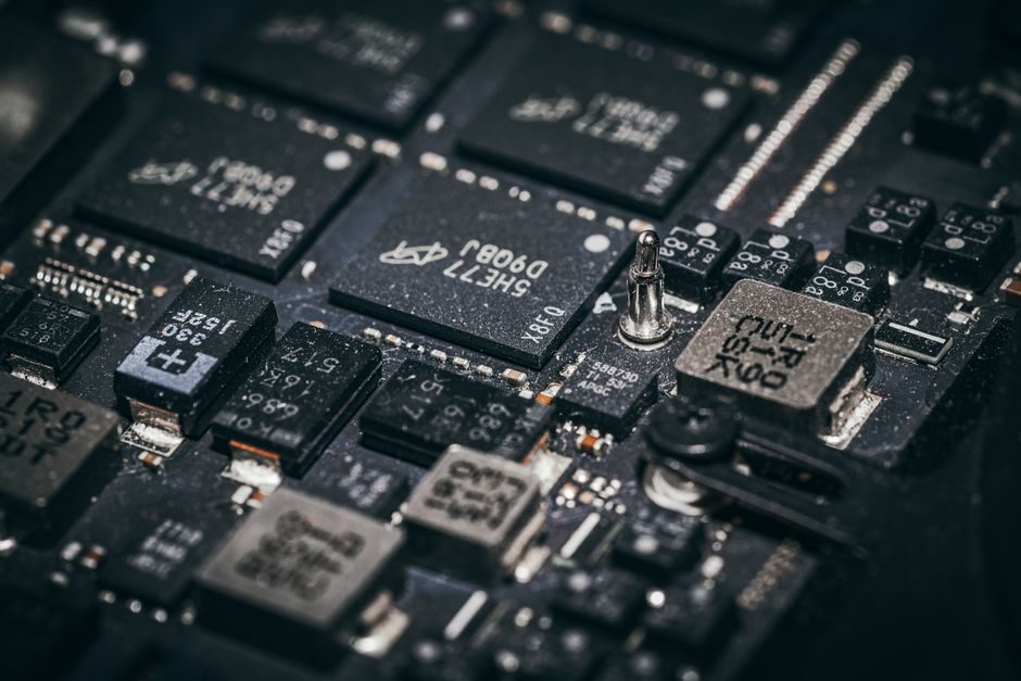
A semiconductor production line is a typical complex manufacturing system integrating more than a dozen types of equipment and running over a dozen product mixes concurrently, where the dispatching strategy directly determines each tool's queue length, each lot's waiting time, and the line's overall operating efficiency [S3].
Design scope covers wafer inspection, laser-assisted bonding, soldering of flip-chip and similar high-density packages, plus annealing, dicing, and final test — every node is sensitive to thermal budget, particulate class, and cycle-time variance.
Line Architecture and Module Boundaries
Wafer-inspection cells pair prober stations with diode-laser beam sources for optoelectrical quality control, while laser-assisted bonding cells are typically specified for flip-chip and high-I/O packages where conventional reflow cannot hold the thermal envelope [S1].
Diode-laser beam sources have been standard in semiconductor production since the 1990s, originally deployed for component marking and laser soldering and progressively extended to wafer prober inspection and laser-assisted bonding of complex packages [S1]. Each functional block runs an independent WIP buffer, and the line-level scheduler must arbitrate tool access across competing product mixes [S3].
For greenfield design, buyers should map each block against cycle-time target, MTBF, and cleanroom class before sizing the inter-block transport — see the broader semiconductor manufacturing cost breakdown framework for how each module consumes wafer, mask, and packaging budget.
Scheduling and Dispatching: Where the Real OEE is Won or Lost
Performance indexes on a semiconductor line are highly cross-correlated: queue length at one tool becomes waiting time at the next, and a single bad dispatch rule can propagate as a global OEE drop of several percentage points within one shift [S3]. Pan, Zhou, and Qiao's IEEE T-ASE survey of cluster-tool scheduling remains the most cited reference for re-entrant tool behaviour, while Mönch, Fowler, and Dauzère-Pérès catalogue the open problem set across photolithography, batching, and dispatching (2025-08) [S3].
Three scheduling families dominate published practice: fuzzy Petri-net reasoning for rule-based dispatch (Shi, Qiao, Ma 2009), multi-agent dynamic dispatch for distributed decision (Wang, Lu 2007), and SVM-driven or data-driven dynamic dispatch for high-mix environments (Ma, Qiao 2015; Wu, Ma 2015) [S3]. Cao et al. (2008) apply TOC-based dynamic hierarchical planning to handle bottleneck shift under variable order mix [S3].
Lee and Jiang's multiple-objective real-time dispatching formulation (2009) treats cycle time, WIP level, and due-date tightness simultaneously rather than optimising one at the cost of the others — the approach is now standard reference in dispatching literature (2025-08) [S3].
Laser Processing Cells: Spec Map
Diode-laser cells in semiconductor lines are typically built around high-power direct-diode or blue-diode sources with homogenizing or multi-spot optics, depending on whether the application is soldering, annealing, or inspection [S1]. Beam-shaping categories used on these lines include welding, brazing, cladding, and homogenizing optics; multi-spot and ultra-wide-spot configurations support large-area anneal and selective solder processes [S1].
Wavelength choice is driven by material absorptivity: blue-diode sources (around 450 nm) are favoured for copper annealing and gold-tin brazing where IR reflectivity is high, while 9xx nm direct-diode sources cover most soldering and selective heat-treatment tasks [S1]. Wafer-level inspection and prober-integrated laser stations are typically specified at lower power with tightly homogenized spots to avoid wafer damage.
Typical field-deployment optics families referenced in vendor documentation include welding, brazing, cladding, and homogenizing optics under the modular OTS family, plus compact/lightweight OTC optics for inline integration [S1]. Buyers should align cell-level optical specification with cleanroom class, throughput target, and the upstream/downstream tool's cycle-time budget before locking the cell layout.
Selection Criteria and Option Comparison
For a greenfield or expansion line, four decision criteria dominate the equipment shortlist: cycle-time stability under high-mix, dispatching-rule adaptability, laser-source compatibility with the package thermal budget, and cleanroom/utility footprint [S1][S3]. Below is a criteria-based comparison of the main line-design options a process engineer will typically weigh.
Fuzzy Petri-net dispatching (Shi 2009) versus SVM-driven dispatching (Ma 2015) versus TOC hierarchical planning (Cao 2008): on rule transparency, fuzzy Petri-net is highest; on adaptability to order-mix churn, SVM-driven is highest; on global bottleneck shifting, TOC is highest; on implementation effort, fuzzy Petri-net is lowest (2025-08) [S3].
Diode-laser source (broadly usable since 1990s) versus blue-diode laser (preferred for Cu/Au) versus flash-lamp anneal (legacy, high-throughput): on copper-anneal efficiency, blue-diode is highest; on legacy silicon compatibility, diode-laser remains broadly usable; on throughput per cell, flash-lamp anneal still leads but at higher utility cost [S1].
Limitations, Failure Modes, and Constraints
Two structural constraints define the upper bound of any line design: WIP imbalance between equipment groups, and the re-entrant behaviour of cluster tools that makes simple FIFO dispatching unstable under high-mix [S3]. Mönch et al. flag scheduling under uncertainty as the dominant open problem in semiconductor operations research, with batching, dispatching, and lot-size interaction still unresolved for sub-7 nm nodes (2025-08) [S3].
Laser-cell limitations are dominated by thermal-budget coupling: a poorly timed laser anneal upstream shifts downstream Cu grain growth, and an undersized homogenizing optic creates non-uniform soak that fails inline four-point-probe tests [S1]. Immunity-based management systems have been proposed in the literature specifically to compensate for equipment breakdown and WIP unbalance that classical expert-system approaches cannot handle (2025-08) [S4].
Buyers specifying new lines should treat dispatching-rule software, laser-cell optical configuration, and inter-block buffer sizing as a coupled set, not three independent purchase orders — a change in any one shifts the line's effective OEE by 2-5 percentage points in published case studies (2025-08) [S3].
Standards, Sourcing, and Buyer Reference
Line design typically references SEMI E10, E84, and E87 for equipment automation and state model, plus IEC 61241 for any laser cell that may be deployed in a powder-handling environment; the dispatching and quality literature is anchored in IEEE T-ASE scheduling surveys and J. Scheduling's 14(6) 2011 problem catalogue (2025-08) [S3].
Buyers should cross-reference the semiconductor manufacturing quality standards map when locking inspection-cell spec, and the NAND flash supply chain 2026 note when the line is being scoped for memory output. For cleanroom envelope, the precision air conditioning 2026 spec map defines the upstream utility envelope the line must fit within.
Trackable signals: dispatching-rule revision notes (fuzzy Petri-net vs SVM vs multi-agent) and laser-cell optics family (modular OTS, compact OTC, multi-spot) are the two line-design variables most likely to shift the published performance index correlation in the next 12 months [S1][S3].
For component-level specifications, see molding line, automatic molding line, and conveyor sorting line.