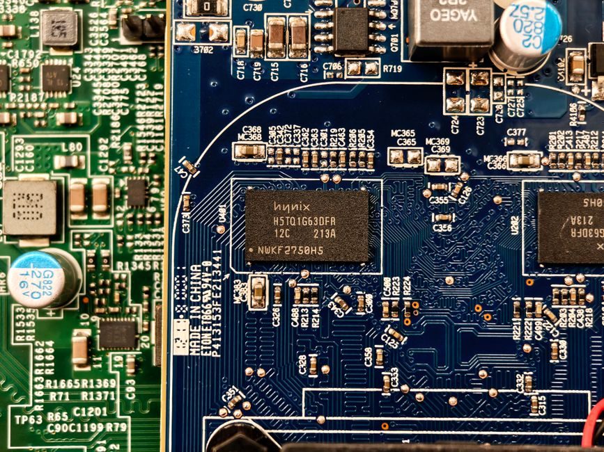
A complete semiconductor bill of materials is dominated by four buckets — wafer fabrication, photomask sets, advanced packaging, and final test — with leading-edge 3 nm/2 nm wafers commonly running into the four-figure-to-low-five-figure USD range per processed wafer, while EUV and High-NA EUV mask sets push mask costs above $50 million per full set [S1][S2].
Cost is a function of process node, lithography wavelength, wafer diameter, die size, package type, test coverage, and qualified volume; fab equipment capex (lithography, etch, deposition, CMP, metrology) is amortised across wafers, while mask and design costs are amortised across units shipped [S1][S2][S8].
Wafer Fabrication: The Single Largest Variable Cost
Wafer fab cost is the dominant share of the ASIC/IC cost stack and scales with node, wafer diameter, and step count — mature 28 nm nodes on 300 mm wafers process at a small fraction of the cost of 3 nm/2 nm wafers that require EUV and High-NA EUV layers [S1][S2]. A leading-edge fab producing sub-3 nm logic runs hundreds of sequential steps with near-perfection yield requirements, and each added EUV layer increases cycle time, gas/photoresist consumption, and tool depreciation per wafer [S2][S9].
The 300 mm wafer format is the industry baseline for advanced logic, memory, and most analog/mixed-signal production; 200 mm remains common for analog, MEMS, RF, and power devices, where tooling and process maturity keep per-wafer cost well below 300 mm advanced nodes [S1][S7]. Cost per wafer is governed by tool depreciation (EUV scanners in the high-hundreds-of-millions USD class), chemicals, gas, ultra-pure water, photoresist, cleanroom operating cost, and labour — and a fab equipment operating-lease structure is a recognised lever to lower balance-sheet exposure on lithography and deposition tools [S8].
Photomask Cost: The Hidden Fixed-Cost Driver
Mask set cost is a front-loaded non-recurring engineering (NRE) line that can exceed the per-unit die cost for low-volume parts — High-NA EUV mask economics were an explicit industry concern in mid-2026, with EUV and High-NA EUV adoption decisions driven by amortised mask cost across expected wafer volume [S2]. Each mask level is a precision substrate of chrome-on-quartz (or equivalent low-thermal-expersion material for EUV) requiring e-beam or laser writing, inspection, and pellicle integration; the number of mask levels scales with metal and via stacks and is the main reason a 2 nm logic mask set costs several times a 28 nm set.
Mask cost is amortised across units shipped, so the crossover volume where NRE is paid back depends on mask set price, wafer cost, and packaging/test — for a $30M mask set amortised over 1 million units, mask contributes roughly $30 per die before yield, which is why mask-intensive leading-edge parts struggle economically at low volume [S1][S2].
Packaging and Assembly: Where Cost Has Shifted Upstream
Advanced packaging — including flip-chip BGA, 2.5D silicon/glass interposer, fan-out wafer-level packaging (FOWLP), and 3D hybrid bonding — is now a first-class cost line rather than a back-end afterthought, with chiplet architectures and HBM stacks adding integration cost that historically sat on the wafer [S2]. Panel-level packaging entered its second wave in 2026, with engineering reality (yield, panel handling, substrate availability) shaping the cost curve versus 300 mm wafer-based advanced packaging [S2].
TSV (through-silicon via) complexity has been flagged as a manufacturing bottleneck in 2026, and HBM4 reportedly stuck with microbumps and postponed hybrid bonding — both are direct packaging-cost decisions that propagate to memory and logic system cost [S2]. Plastic and high-purity thermoplastic components (PPS, PEEK, PVDF) are used throughout fab and packaging tools for chemical, plasma, and thermal compatibility, contributing to tool and consumable cost [S7].
Test and Quality: SPC, MES, and the Cost of Defectivity
Test cost scales with pin count, test time per part, and the depth of structural and functional coverage — wafer-probe plus final test together typically add a single-digit USD figure per part for digital logic and a larger share for analog, mixed-signal, and RF devices [S2][S3]. Wafer probe itself is under pressure in 2026 as multi-die assemblies shift known-good-die economics, with probe cards, probe needles, and contactor maintenance adding recurring cost lines [S2].
Manufacturing Execution Systems (MES), Statistical Process Control (SPC), Engineering Data Collection (EDC), and traveler/router-based WIP tracking are now baseline cost-of-quality infrastructure, with traveler-based MES providing configurable lot tracking, holds, and ERP integration at a fraction of the price of full-stack MES [S3]. Event-driven reinforcement learning for long-horizon fab control, vision-language models for lithography defect detection, and graph-attention virtual metrology (Intel Foundry, ASU) are 2026 R&D directions that target defectivity cost directly [S2].
Total Cost of Ownership: Materials, Energy, PFAS, and Tool Lifecycle
Total cost of ownership extends past per-wafer and per-die lines into chemicals, ultra-pure water, gas, energy, and tool lifecycle — photoresist and rinse chemistries have historically relied on PFAS, and imec's 2025 PFAS-removal work signals that future fabs will face reformulation cost and qualification cycles as PFAS is phased out of resist and rinse stacks [S4]. FPD and adjacent process control (HORIBA-class gas/liquid composition and particle detection) is also a measurable operating cost line for any line transitioning between display and wafer-type processes [S5].
Tool matching, preventative maintenance scheduling, and equipment history tracking — all core MES functions — are direct TCO levers because unplanned tool downtime at advanced nodes is a larger revenue loss than the maintenance spend itself [S3]. Operating leases on semiconductor manufacturing equipment (lithography, deposition, etch) are a financing structure used to lower the all-in cost of tool ownership and keep assets off balance sheet, particularly relevant for sub-fab capex control [S8].
Cost Comparison: Mature Node vs Advanced Node vs Advanced Packaging
The cost trade-off between mature and leading-edge nodes is dominated by mask NRE, wafer cost, and packaging/test — a 28 nm 300 mm wafer is a small fraction of the cost of a 3 nm wafer, but a 2 nm mask set is multiple times the cost of a 28 nm mask set, so the crossover where advanced-node die becomes cheaper than mature-node die is highly volume-dependent [S1][S2]. High-NA EUV adds per-wafer lithography cost and per-mask cost; the economic case hinges on multi-patterning reduction, yield, and wafer volume, and High-NA EUV is currently a 2026 mask-economics discussion topic rather than a blanket recommendation [S2].
For mixed-signal, power, RF, and MEMS designs on 200 mm, mature-node wafer plus standard QFN/BGA packaging plus digital/analog test is the lowest-cost path and remains the right choice for low-to-mid volumes [S1][S7]. For chiplet, HBM, and 2.5D/3D heterogeneous integration, advanced packaging cost can rival or exceed wafer cost on a per-system basis, so the cost optimisation target shifts from lithography to interposer, microbump/hybrid bonding, and known-good-die test yield [S2]. Foundries continue to act as a capacity gate at the leading edge, with leading-edge capacity rationing affecting who competes at sub-3 nm and indirectly influencing per-wafer price [S2].
Decision Criteria: When to Specify Which Cost Stack
Pick a mature node (≥28 nm) when design constraints are analog/RF/MEMS, volume is below several million units, or the BOM is dominated by packaging and test rather than silicon area — the lower mask NRE and lower per-wafer cost keep all-in unit cost predictable [S1][S7]. Pick an advanced node (≤5 nm) only when power, performance, or area cannot be met at a mature node and volume is high enough to amortise mask NRE across shipped units — EUV/High-NA EUV layers are the cost pivot, and High-NA EUV adoption is justified when multi-patterning reduction and yield gains outweigh higher mask and tool cost [S2].
Pick advanced packaging (2.5D interposer, FOWLP, 3D hybrid bonding) when the system is bandwidth-limited (HBM, networking, AI accelerators) and chiplet partitioning yields a better cost-yield curve than a monolithic die, but only after modelling interposer, microbump, and known-good-die cost alongside silicon cost [S2]. Pick standard packaging (QFN, BGA, WBBGA) when the design is single-die and cost is dominated by PCB and test — packaging becomes the cost pivot, and panel-level packaging may shift that cost curve in 2026–2027 for high-volume consumer parts [S2]. For cost-driven sensor and process-control integration into a fab line, specifying the right flow meter and pressure transmitter on gas and chemical lines is a direct TCO lever because metrology drift and unplanned calibration drive yield loss.
Standards, Sourcing, and Sourcing-Side Cost Levers
Process and quality standards that govern cost-of-quality lines include the GEM300 and gRPC interface stack driving Industry 4.0 fab integration, ISA-95-style MES/ERP integration patterns, and traveler-based WIP with SPC/EDC — these are cost levers, not just compliance items, because they directly reduce excursion cost and yield loss [S3]. Sourcing-side cost levers include multi-vendor mask data prep, qualified second-source packaging subcontractors, and operating-lease structures on lithography and deposition tools, all of which have been used to lower all-in fab cost in 2026 [S8].
For comparison with adjacent industrial cost stacks — dynamic compactors, angular-contact bearings, capping/sealing machines — the same NRE vs volume trade-off applies, and a semiconductor capacity planning stochastic model is the right starting point when fab throughput is the binding cost constraint [S2]. For the 2026 quality-standards landscape governing cost-of-quality, the semiconductor manufacturing quality standards spec map is a useful reference, and Industry 4.0 adoption (GEM 300, gRPC) directly determines MES integration cost across 2026 builds. Trackable 2026–2027 cost signals: High-NA EUV mask-economics adoption decisions, panel-level packaging second-wave yield ramp, HBM4-to-hybrid-bonding transition, and PFAS reformulation of photoresist/rinse stacks [S2][S4].
For the relevant spec sheets and selection criteria, see additive manufacturing material.