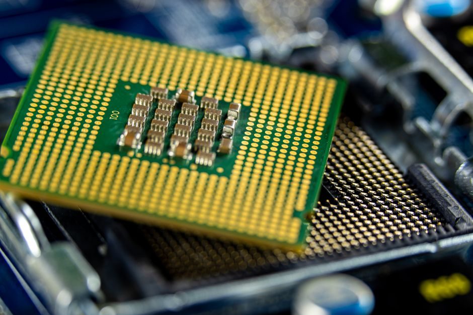
A 1,000-die budget run on GlobalFoundries' 180 nm GF180MCU process is being offered at $2,000-$7,000 depending on slot size and pricing tier, putting per-die silicon cost between $2.00 and $7.00 before packaging [S3].
The number that matters in a real BOM, however, is not the raw wafer substrate price but the cumulative cost of masks, wafer processing, yield, dicing, packaging, and test — and these scale sharply with process node and wafer diameter rather than with the silicon itself [S1][S2].
What "Wafer Cost" Actually Buys
A semiconductor wafer is the substrate on which transistors and interconnects are etched or deposited to form integrated circuits, and the term covers silicon, GaAs, SiC, GaN, and other single-crystal or poly-crystalline materials used across logic, memory, MEMS, and power devices [S2]. The starting blank wafer is a single line item in the cost stack; the lithography, etch, implant, CMP, and metallization steps that follow are the dominant cost drivers for any node at 65 nm and below [S1].
Industry cost models consistently split a finished die into wafer fab, packaging, and test buckets, with fab cost typically outweighing the other two combined for advanced nodes — packaging and test can become the larger share only at mature nodes (180 nm and above) and at small die sizes where back-end labour dominates [S1]. For a fabless buyer, the relevant unit is therefore the packaged, tested die price quoted by the foundry or assembly house, not the polished wafer price.
Cost Drivers Ranked by Impact
Mask set cost is the single largest non-recurring expense for any new product tape-out and scales roughly with node complexity: a mature 180 nm mask set is an order of magnitude cheaper than a 7 nm mask set, which industry sources put in the multi-tens-of-millions range [S1]. Wafer diameter — 150 mm, 200 mm, or 300 mm — moves the die-per-wafer count by a factor of ~3-4x between adjacent generations, so even small per-wafer price differences compound across the reticle field [S1].
Yield is the second-order driver: a 5-percentage-point yield swing on a high-value wafer can swing gross margin by more than 10 points, and yield itself depends on die area, redundancy strategy (laser repair, ECC, spare rows), and process maturity [S1]. Packaging tier — QFN, BGA, wafer-level chip-scale package (WLCSP), 2.5D/3D — adds $0.10 to several dollars per die and is where assembly backlogs and substrate shortages show up first in cost [S4]. Test cost, including ATE time and any system-level burn-in, is small in dollars but a hard floor that does not scale down with die size.
MPW vs Full-Wafer Cost: Real Numbers

Multi-project wafer (MPW) shuttle pricing is the cheapest path to working silicon for prototypes and low-volume runs, and wafer.space's published GF180MCU Run 3 schedule (1 August 2026 campaign open, 30 September 2026 early-bird close) lays out a clean comparison [S3]:
- 1×1 slot, 3.93 × 5.12 mm die (20.12 mm² usable), 56 default I/O: $7,000 early bird, $8,000 standard, 1,000 dies per slot [S3].
- 0.5×1 slot, 1.94 × 5.12 mm die (9.93 mm²): $4,000 early bird, $5,000 standard, 1,000 dies per slot [S3].
- 0.5×0.5 slot, 1.94 × 2.53 mm die (4.9 mm²), 48 I/O: $2,000 early bird, $3,000 standard, 1,000 dies per slot [S3].
At $2/die on the quarter slot, the per-mm² cost works out to roughly $0.41, which is a useful sanity check against custom foundry quotes — mature-node MPW should sit in the $0.20-$0.80/mm² band once mask amortization is included [S1][S3]. Full-wafer (dedicated) runs at the same node remove the MPW area discount but add volume leverage: a 200 mm wafer running ~1,500 good dies at similar per-die cost gives the same unit economics with the trade-off of a larger upfront mask and NRE commitment [S1].
Wafer Diameter and Die-per-Wafer Math
Bigger wafers do not reduce per-die cost in isolation — they reduce it through better tool throughput and amortization of fixed photolithography overhead, which is why the 200 mm → 300 mm transition is a per-die cost event, not a per-wafer cost event [S1]. For a 200 mm wafer at 180 nm, the usable die count for a 5 × 5 mm part sits around 1,400-1,500; the same die on 300 mm yields roughly 3,200-3,500, which is why foundries price 300 mm wafers at a premium but quote lower per-die cost on volume [S1].
For procurement teams, the takeaway is that quoting "wafer cost" without specifying diameter, reticle size, and die area is meaningless — a vendor quoting "$X per wafer" for a 150 mm part is not comparable to a "$Y per wafer" 300 mm quote once die-per-wafer is applied [S1][S2]. Use a die-per-wafer calculator to normalize, or ask the foundry for a packed-die yield map at your exact die size before comparing.
Packaging, Test, and Back-End Cost Stack

Back-end cost has two distinct components: assembly (package type, lead frame vs laminate substrate, bond wire vs flip-chip) and test (wafer probe, final test, system-level test, burn-in) [S4]. A QFN assembly on a 180 nm part typically runs $0.05-$0.20 per device at MPW volumes; flip-chip BGA with laminate substrate can run $0.30-$1.50 depending on ball count and substrate layer count [S1]. Wafer-level chip-scale packaging collapses assembly and test into a single line and is preferred for small die where substrate cost dominates, but it requires a clean fab back-end and is not offered on every mature node [S1].
Test cost is a function of ATE pin count, test time per part, and the number of test insertions. Analog-heavy mixed-signal parts typically pay a test-time penalty because of DC and AC parametrics; a digital-only part at 180 nm can complete final test in under a second on a low-pin-count handler [S1][S3]. Buyers should ask vendors for test time separately from the package quote — a 4-second test vs a 0.5-second test at the same handler rate is a 8x swing in ATE amortized cost per part.
Where Budget Quotes Break Down
The $2/die MPW number is real but bounded: it assumes a 180 nm mixed-signal process, 1,000-die volume, and a customer willing to ship a clean GDS by 16 December 2026 with parts delivered in Q2 2027 [S3]. It does not include IP licensing, custom I/O pad ring generation, Chip-on-Board packaging add-on, or the cost of a second tape-out if the first fails — and at 180 nm without redundancy, a respin is the norm rather than the exception for any non-trivial design [S1][S3].
For procurement teams scoping a real project, the honest cost benchmark is packaged-tested-die cost, not wafer cost, and it should be modeled at three volumes: 1k (MPW prototype), 10k (early production), and 100k+ (mass production). Each tier brings a different cost stack: MPW is mask-amortization-bound, early production is yield-bound, mass production is back-end-bound [S1][S4]. A vendor who quotes only one of these tiers is not quoting a production-ready part.
Standards and Sourcing Constraints
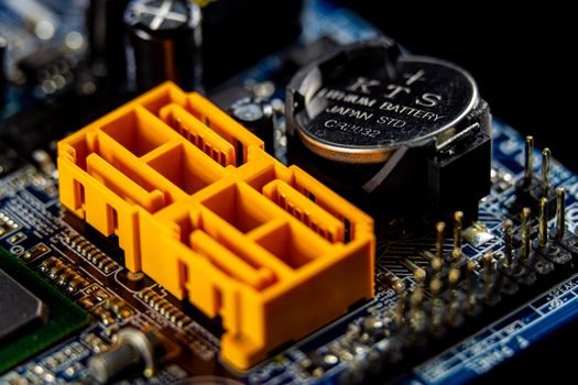
Wafer-level quality is governed by SEMI standards (notably SEMI M1 for silicon wafer specifications and SEMI MF on dimensional metrology), and buyers should ask for a wafer specification sheet — not a generic "prime wafer" claim — because resistivity, surface metal contamination, flatness, and bow directly affect downstream yield [S2]. For power-device wafers (SiC, GaN), the relevant substrate specs are different again and are covered under SEMI M55 (SiC) and related documents; the silicon-carbide encyclopedia entry covers how substrate cost dominates total epi-ready wafer cost in that family.
For foundries running mature nodes like the 180 nm GF180MCU process used by wafer.space, the practical sourcing constraint is shuttle timing rather than capacity — MPW slots close on fixed dates, and missing the submission deadline pushes the project by a full quarter [S3]. Lead-time discipline matters more than unit price at this scale: a $1/die cost saving on paper is erased by a single missed shuttle.
Who This Cost Model Is For — and Who It Is Not
The MPW cost stack described here is built for low-to-mid volume ASIC prototyping, university tape-outs, and mixed-signal IC startups shipping under 100k units per year — the same customer profile that uses 180 nm and 350 nm processes for power management, sensor interfaces, and analog-heavy SoCs [S1][S3]. A buyer running a 7 nm mobile SoC at 50 million units per year is in a completely different cost regime, where mask amortization, advanced packaging (FoWLP, 2.5D CoWoS), and HBM stacking dominate the per-die cost stack [S1].
It is also not the right model for commodity discretes or memory, where wafer fabs optimize for die density and bit cost rather than per-die packaged price — a DRAM wafer is sold by the gigabit and an IGBT wafer by the ampere, not by the packaged unit [S1][S2]. If your product is a power device, the comparison chart should be $/A or $/mm² of active area, not $/die. For a wider cross-material view of how substrate choice shifts cost in adjacent process families, the silicon-nitride encyclopedia entry and silicon-steel entry show how non-IC silicon-bearing materials fit into a similar cost-driver framework for ceramics and electrical steel respectively.
Side-by-Side: MPW Tier vs Volume Tier on Cost Drivers
Comparing the three MPW slot sizes from the GF180MCU Run 3 schedule against a hypothetical 100k-unit production run on the same node, four cost criteria stand out [S1][S3]:
- Per-die cost: $2.00-$7.00 on MPW (1,000-die lot) vs single-digit cents to low tens of cents on full-wafer volume runs, depending on yield and back-end.
- Mask NRE: Amortized across 1,000 dies on MPW vs 1 million+ dies on volume — a $500k mask set is $500/die at MPW and $0.50/die at volume.
- Lead time: 6-9 months on a published MPW shuttle (Q2 2027 ship from 1 August 2026 campaign open) vs 4-6 months for a dedicated wafer start, but with a higher tape-out risk if the GDS is not clean [S3].
Total Cost of Ownership Beyond the Wafer
Real landed cost of a finished IC is wafer fab + assembly + test + IP royalty + qualification + yield loss + logistics + inventory carrying [S1][S4]. A buyer who only tracks the wafer line item will underestimate the all-in number by 30-60% on a mature-node mixed-signal part, and by 10-20% on a digital-heavy advanced-node part, depending on how much of the cost stack is hidden in IP and qualification rather than the foundry quote [S1].
For engineering procurement, the cleanest way to get a defensible cost model is to ask for a packaged-tested-die price at three volumes, with IP royalty shown as a separate line and a written yield assumption attached. If a vendor refuses to break out packaging from test, or refuses to give a volume-tier quote, treat the MPW number as a prototype benchmark and budget separately for production escalation [S4]. For related cost-driver work in adjacent industrial categories, the stainless steel grade selection map for construction projects uses the same driver-rank-then-compare framework for a different material family, and the copper OEM vs ODM decision map is a useful parallel for how MOQ and IP shape landed cost in metals sourcing.
Watch the 30 September 2026 early-bird deadline for GF180MCU Run 3 and the 9 December 2026 final purchase deadline as the next concrete signals for buyers locking in 2027 prototype silicon [S3].