Worldwide silicon wafer revenue re-accelerated in 2024 after the 2023 down-cycle, with the 2024 figure cited in industry trackers at roughly USD 11.4 billion [S7] — a baseline that frames every 2026 forecast revision.
For procurement and process engineers the 2026 question is not "is the market growing" but "which diameter / node / surface-finish tier is tight, and which is oversupplied," since 300mm polished and epitaxial wafers behave as a different commodity from 200mm and 150mm. The same 2026 cycle that lifted silicon carbide power-device substrates also lifted the underlying mono-crystalline silicon upstream, so the two demand curves partially correlate [S5].
2026 Market Sizing and the 2025-2030 Trajectory
Industry trackers converge on a 2026 global silicon wafer market value in the USD 13-15 billion band, with mid-single-digit to low-double-digit CAGR through 2030 [S7] (2025-11). The trajectory is asymmetric by diameter: 300mm wafer demand grows fastest because advanced logic (3 nm/2 nm GAA, sub-2 nm back-side power), HBM4 base die, and image-sensor CIS all consume 300mm area, while 200mm stays roughly flat as mature-node automotive, industrial, and pressure transmitter / flow meter analog ICs dominate that mix.
150mm and smaller diameters, used in legacy power discretes and some MEMS, remain a structural niche — relevant for sourcing but not for tonnage forecasts.
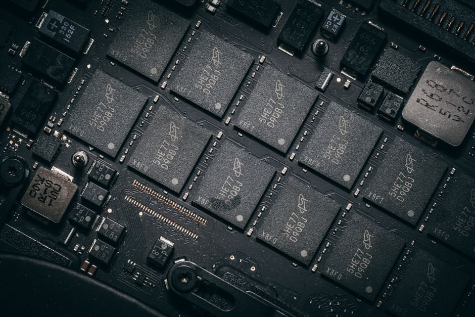
Diameter, Node and Surface-Finish Tier Comparison
For engineering selection, the 2026 wafer market breaks into four tiers, each with its own pricing, lead-time and qualification gate: [S1]
1) 300mm polished (P-type, B-doped, 1-100 Ω·cm) — used for logic, memory, CIS. Largest volume; 8-12 week contract lead time; price benchmark ~USD 100-130 per wafer depending on edge profile and particle spec.<br>2) 300mm epitaxial (P/P-, 2-10 µm epi on graded or abrupt buried layer) — required for advanced logic, image sensors, and high-voltage CMOS; typically quoted at 20-30% above polished 300mm.<br>3) 200mm polished / epi — mixed bag of automotive MCUs, power discretes, MEMS, and analog. Prices softer than 300mm but lead times can extend under auto-AOIs.<br>4) 150 mm and below — power MOSFET, IGBT and industrial valve sensor legacy nodes; small volume, often MOQ-constrained, frequently sourced from Chinese producers.
The first two tiers dominate revenue; the latter two matter for sourcing coverage rather than headline market size [S7] (2025-11).
Capacity Geography and Supplier Tier

Global 300mm polished and epi capacity remains a five-supplier market: Shin-Etsu, SUMCO, GlobalWafers, Siltronic, and SK Siltron together account for the dominant share of merchant supply (qualitative, consistent across industry coverage) [S7] (2025-11). Chinese entrants (NSIG, ZJSemi, MCL, TDG) have material 200mm and 150mm share and growing but still minority 300mm presence; for procurement they matter most on legacy diameters and as a price-discipline lever.
Geographically, Japan, Taiwan, Germany, South Korea and the United States host the majority of large-diameter ingot growth and wafering lines. The U.S. CHIPS-funded build-out of TSMC Arizona, Samsung Texas and Intel Ohio adds 300mm demand without proportionally adding merchant wafer supply, so the 2026-2028 setup is structurally tight on 300mm epi in particular [S7] (2025-11). Procurement should expect wafer allocation, not spot-market pricing, to govern 300mm contracts through 2027.
Adjacency: SiC, GaN and the Silicon Upstream Linkage
Silicon carbide substrates (150mm and the early 200mm pilot lines) are a separate commodity, but the upstream poly-silicon supply chain, crystal-growth furnace set, and cleanroom wafering know-how overlap with the silicon wafer industry [S5] (2026-06). That overlap is why 2026 SiC fab announcements from Wolfspeed, ROHM, Infineon and onsemi pressure the same quartz and high-purity gas supply lines that feed silicon ingot growth, even though SiC boules are grown by PVT on dedicated SiC seeds rather than Czochralski silicon pulls.
For a process engineer, the practical consequence is dual-qualifying suppliers across silicon carbide epi and silicon 300mm epi where the same fab consumes both — a real scenario in traction inverter and onboard-charger lines that pair SiC MOSFETs with silicon gate-driver and iso-rail ICs.
Standards, Spec Discipline and Sourcing Gates

Wafer procurement is governed by SEMI standards on dimensional and surface metrology (SEMI M1 for silicon wafer diameter/thickness, SEMI MF on flatness and surface finish) and by customer-specific qual such as the Zero Defect / ppm-defect gate at leading foundries. For 300mm epi, resistivity uniformity, slide-mark density, and LLS (light-scattering defects) are the metrics that drive acceptance, not headline wafer price [S7] (2025-11).
Practical 2026 sourcing gates: (a) confirm SEMI M1 revision cited on the certificate of analysis; (b) require 9 mm or 12 mm notch / flat per SEMI M1; (c) for epi, require thickness and resistivity maps, not just nominal; (d) lock multi-year volume agreements for 300mm because spot capacity in 2026 is thin; (e) on 200mm and below, dual-source a Chinese merchant as a price hedge.
Failure Modes and What Goes Wrong in Tight Markets
Three failure modes repeat in tight wafer cycles: (1) particle excursion on a new ingot growth run that delays 300mm epi shipments; (2) edge-chipping during automated FOUP handling that scrapes yield at the customer fab, not at the wafer maker; (3) resistivity drift on P/P- epi used in image sensors, which only shows up at probe after several process steps. None of these show up in headline market-size tables, but all three govern 2026 delivery risk [S7] (2025-11).
For procurement, the mitigation is contractual: pre-defined excursion response time (typically 72 h), 8D root cause within 10 working days, and a documented engineering-change procedure for any ingot / puller re-qualification. Wafer contracts in 2026 that omit these clauses are exposed.
The 2026 silicon wafer market is best read as a tight 300mm epi cycle inside a structurally growing semiconductor wafer industry that also pulls SiC substrates into the same upstream bottleneck. The next verifiable nodes to watch are the SUMCO and GlobalWafers Q2 2026 billing updates, the TSMC Arizona N3 wafer-out milestone, and any 200mm SiC pilot line commissioning from Wolfspeed Mohawk Valley — all trackable signals for whether 300mm tightness extends into 2027.
For related coverage, see Taper Bush 2026 Buying Guide: Bore, Material, Standards and Sourcing Levers.