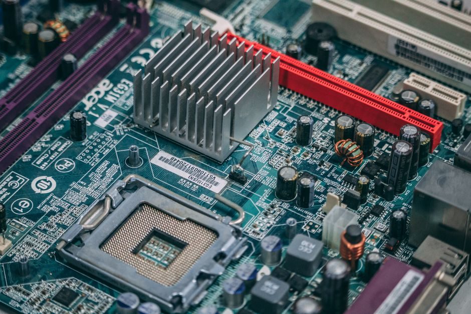
A silicon wafer production line is a sequence of crystal-growth, slicing, surface-finishing, and cleaning cells sized to a target diameter (8 in / 200 mm or 12 in / 300 mm), a monthly wafer count, and a cleanroom class. The reference throughput is the 8 in / 12 in line at Hangzhou Zhongxin Wafer Semiconductor, which targets 350,000 wafers/month at full ramp with a first-stage 12 in capacity of 30,000 wafers/month and a planned 200,000-wafer expansion [S2].
Process flow is fixed by the physics of single-crystal silicon: ingot heat treatment repairs neutron or thermal-donor damage before slicing, then wire sawing replaces blade cutting for higher kerf yield, followed by lapping, CMP polishing, and final cleaning [S6]. Equipment choice and cleanroom classification govern everything downstream, including layout length, FOUP/reticle handoff points, and slurry-recovery loops.
Core Process Stages and Engineering Inputs
The canonical process chain reviewed in current literature covers ingot heat treatment, X-ray orientation check, cutting/slicing, lapping, polishing, cleaning, and packaging [S6]. Blade cutting is being displaced by wire sawing because the wire process holds kerf loss to roughly the wire diameter (typically 100–180 µm) and supports batch cutting of hundreds of wafers per run, while older blade ID saws are limited to single-wafer cuts.
Heat treatment before slicing is used to eliminate thermal donors and to repair neutron-irradiation damage; the X-ray diffraction step then confirms crystal orientation to within ~0.5° before wafers are indexed for cutting [S6]. For a 300 mm line, post-CMP cleaning must hit particle adds below the SEMI M1 surface-finish envelope used as the de-facto prime-wafer reference, which dictates the wet-bench chemistry (SC1 / SC2 / dilute HF) and the megasonic transducer power density.
Line Sizing: 8 in vs 12 in Throughput Targets
The 8 in / 12 in dual line at Hangzhou Zhongxin is engineered for 350,000 wafers/month combined at ramp, of which 30,000 wafers/month is the initial 12 in envelope, with a 200,000-wafer 12 in expansion planned [S2]. Construction ran 20 months (one year and eight months) from groundbreaking to the November 2019 completion ceremony, with a further equipment-and-process debug window before 12 in mass production [S2].
For 200 mm-only lines, the 350,000-wafer figure maps to roughly 24–28 ingots/day at typical 1,500 mm Czochralski pull lengths and 95% slicing yield, while 300 mm-only lines at the same wafer count need larger-diameter hot zones and longer crystal pullers. The 12 in hot zone requires CZ pullers with ~32-inch crucible capacity, magnetic-field (MCZ) option for oxygen control below 14 ppma (the typical prime target for logic-grade wafers), and a hot-zone lifetime rated for 200+ hours between rebuilds.
Cleanroom, Utilities, and Material-Handling Layout
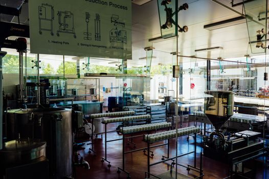
Wafer processing after slicing runs in ISO Class 3 or cleaner zones for prime 300 mm lines, with ISO Class 5 acceptable for some lapping back-end cells; AMHS / OHT tracks typically span the polishing and cleanroom sections to keep FOUPs off the floor. Slurry recycling for CMP must separate ceria or silica solids from the rinse water to keep total organic carbon in the reclaim loop below the fab's UPW feed spec, and the slurry-blend skid is usually co-located with a chemical-mechanical planarization tool cluster. [S6]
Stainless process piping for UPW, slurry, and HF follows the same 304L / 316L grade logic used in semiconductor wet benches, with electropolished interior finishes and orbital welds to keep extractables below 1 ppb at the point of use. For 200 mm lines, stainless steel selection for electronics drives the piping spec, while fab structural steel and equipment frames commonly shift to silicon steel for the lamination cores of the AC process-tool power supplies — see the silicon steel reference for typical M19/M27 grade choices and lamination thickness ranges.
Production vs Pilot: Selecting a Foundry Model
Foundry selection should hinge on wafer count, diameter, and the ITAR / export profile of the end product. A US-based ITAR-registered MEMS foundry with 100% in-house wafer services — two fabs at Medford, OR and Palm Bay, FL — supports defense and export-controlled programs where the full process flow must stay onshore [S5]. A global secondary-market distributor (WaferNet) instead serves equipment makers, universities, and R&D labs that need test, reclaim, and odd-lot inventory at low MOQ [S3].
A 100,000-wafer/month custom line on 8 in (200 mm) is the right scale for specialty MEMS, power devices, and RF; 200,000+ wafers/month on 12 in (300 mm) is the right scale only when the downstream fab is on a logic, memory, or large-area analog process node. For R&D, custom-pattern wafer services and small-batch coated wafers (Thermal Oxide, PETEOS, Nitride, POLY, Cu, W, TiN, TaN, PR) plus 200 / 300 mm Glass wafer and SiC wafer options are listed by current third-party suppliers [S4], and these let a process team qualify a tool or chemistry without buying full-fab inventory.
Reliability, Yield, and Failure-Mode Constraints
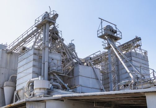
The dominant yield-limiters on a new 12 in line are wire-saw chatter (which lifts wafer TTV above the 10 µm target), CMP dishing on wide copper features, and backside-particle adds in the final clean. Slicing damage depth of 10–30 µm per side must be fully removed by lapping before CMP, and any residual sub-surface damage shows up as haze in a post-clean inspection, which is why lapping stock removal is over-sized to give the polisher a clean starting surface [S6].
Ingot heat treatment to repair thermal-donor damage must be done in a controlled atmosphere with a ramp/soak profile matched to the resistivity target; under-anneal leaves donors that drift under later high-temperature processing, and over-anneal slips the crystal. For prime 300 mm wafers, the upstream crystal growth and downstream fab thermal budget are co-optimized — designers should treat the wafer as a thermal actuator, not a passive substrate.
Standards, Specs, and Sourcing Anchors
Line design should anchor to the SEMI M-series for wafer dimensional specs (M1 for 300 mm prime, M2 for 200 mm prime) and to the per-tool safety standards for the wet benches, slurry skids, and HF handling. Wafer-handling automation (OHT, stocker, FOUP) follows the SEMI E-series interface standards, and process-tool power follows the fab's SEMI S2 / S8 environmental, ergonomics, and electrical-safety envelope. [S1]
Trackable signals to watch over the next two quarters: (1) commissioning milestones of new 12 in capacity that confirm 30,000 → 200,000 wafer/month ramp curves [S2], (2) Industry 4.0 / IIoT retrofit cycles on existing 200 mm lines as older MEMS fabs move to closed-loop process control — see the Silicon Wafer Industry 4.0 adoption 2026 spec map for the fab-floor reality, and (3) capacity-planning decisions on 300 mm thinning and SOI / bonded-wafer variants covered in the Silicon Wafer Capacity Planning 2026 sizing, thinning, and regional build-out brief.
Spec-level background on the components involved: silicon carbide, and silicon nitride.