
Wafer-level vacuum packaging (WLVP) replaces the legacy one-die-at-a-time metal/ceramic vacuum package with a parallel wafer-to-wafer bond, capping every microbolometer die on a wafer in a single bonding cycle before dicing, which is the structural source of the cost reduction [S1][S2][S5].
The bonded cap wafer carries the infrared window, an antireflective or moth-eye/grating structure for over 80% LWIR transmission, a sealed cavity, and in most designs an internal getter, while the sensor wafer carries the suspended microbolometer pixels and the ROIC [S2]. Reported internal pressures span 50 mTorr (about 6.7 Pa) for Cu-Sn SLID builds with nano-multilayer getters [S1], 133 to 533 Pa without getter, and as low as 0.13 Pa with getter in Au-In TLP plus glass-frit designs [S2], all below the less than 10 mTorr operating target for microbolometer focal plane arrays [S5].
Why die-level packaging is the expensive baseline
Traditional die-level packaging dices the MEMS wafer first, then loads each individual die into a separate metal or ceramic vacuum package, evacuates that package through a tubulation or pinch-off, and seals it, so every package has its own vacuum pump-down, getter activation step, and hermeticity check [S2][S5].
The unit cost therefore tracks the per-die tooling, per-die getter, per-die pump time, and per-die yield risk, all of which scale with die count rather than wafer count, and the resulting can packages are also larger and heavier than a wafer-bonded cap [S5][S6]. For consumer-grade thermal imagers this die-level cap has been the single largest cost line item on the bill of materials, which is why the first generation of sub-$1000 thermal cameras is gated on a viable WLVP process [S6].
Bonding routes and their cost-driving trade-offs
Four bonding families dominate WLVP for microbolometers: anodic bonding, fusion bonding, glass frit bonding, and eutectic or SLID/TLP metallic bonding, each setting a different cap on throughput, thermal budget, and hermeticity margin [S2].
Cu-Sn solid-liquid interdiffusion (SLID) bonding, demonstrated by the RTI/Texas Instruments team on microbolometer FPA wafers, is a parallel-process wafer-to-wafer bond that produces a Cu/Cu3Sn/Cu microstructure and is compatible with cap wafers already coated with thin-film getters and AR films [S5]. A low-temperature variant using Cu-Sn with a Zr-Ti-Ru nano-multilayer getter measured package pressure near 50 mTorr with a narrow across-wafer distribution, shear strength suitable for downstream dicing, and was explicitly targeted at microbolometer pixels built on top of a read-out IC, where the IC thermal budget is the constraint [S1]. Au-In transient liquid phase (TLP) bonding has been used to bond a double-side-polished moth-eye silicon wafer to a cavity wafer at low temperature, after which the assembled cap is bonded to the sensor wafer with glass frit at high temperature to thermally activate the internal getter; shear strength averaged 23.38 MPa and He-leak rates reached 0.1 x 10^-9 atm*cc/s per MIL-STD-883 [S2]. A side-by-side read of the three main options against decision criteria a process engineer cares about: (a) bond temperature: Cu-Sn SLID and Au-In TLP run at low temperature and protect the underlying ROIC, glass frit runs at high temperature but is what thermally activates the getter; (b) throughput: all three are wafer-scale and parallel, so per-die bond time is amortized; (c) hermeticity margin: Cu-Sn SLID and Au-In TLP both clear MIL-STD-883 He-leak limits, glass frit is a mature high-yield route; (d) getter integration: Cu-Sn SLID and the Au-In TLP plus glass-frit hybrid both integrate a thin-film or nano-multilayer getter inside the cap, which is what pulls the cavity from 133-533 Pa down to 0.13 Pa in the Au-In TLP paper [S1][S2][S5].
Where the cost actually goes inside a WLVP line
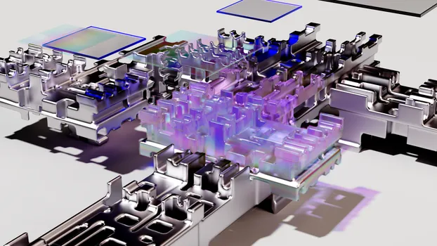
Cap wafer cost is dominated by the IR-transparent silicon, the AR or moth-eye/grating etch, the thin-film getter, and the bonding metallurgy, while the sensor wafer side is dominated by the microbolometer pixel process, the ROIC, and through-cap vias or pad reveal steps [S1][S2][S5].
On a Cu-Sn SLID build, the bond is tuned by three variables (bonding temperature, pressure, and time) that set the Cu/Cu3Sn/Cu intermetallic ratio and therefore both hermeticity and mechanical strength, and the cap side adds a self-aligned shadow-masked Zr-Ti-Ru nano-multilayer getter that survives the high step height of the cavity etch [S1]. On the Au-In TLP plus glass-frit build, the IR window is a separately patterned double-side-polished wafer with sub-wavelength moth-eye or grating features that lift LWIR transmission above 80% without a deposited AR coating, removing both a coating step and a coating-yield term from the cost stack [S2]. Across both routes, the per-wafer tooling (bond aligner, bond chamber, thin-film getter sputter or evaporator, dicing saw) is fixed cost, so spreading it over thousands of cavities per wafer is the mechanical reason a single microbolometer die in a WLVP line ends up cheaper than the same die in a metal can, even before yield is factored in [S2][S5][S6].
Vacuum integrity, getters, and the reliability cost lever
Microbolometer FPAs need an internal ambient below 10 mTorr for optimum sensitivity, and the bonded cap has to hold that vacuum for the operating life of the imager, so the getter is what converts a one-time pump-down into a multi-year stable cavity [S5].
The reported data points line up cleanly: a Cu-Sn SLID wafer with a Zr-Ti-Ru nano-multilayer getter held near 50 mTorr [S1]; an Au-In TLP plus glass-frit wafer with internal getter measured 0.13 Pa internal pressure, while the same construction without the getter sat at 133 to 533 Pa [S2]. That gap is the cost-versus-life lever, because dropping the getter would let the package pressure rise into the 100 Pa range and degrade NETD, but skipping the getter also skips a process step, a sputter target, and a shadow-mask align, so the engineer choice is whether to pay the getter cost to keep the NETD spec over a 10-year automotive or industrial life. Hermeticity is verified by He-leak testing per MIL-STD-883, and the Au-In TLP plus glass-frit build reported leak rates as low as 0.1 x 10^-9 atm*cc/s, a number that is small enough to treat the cavity as effectively sealed for thermal-imager service life [S2]. For a process engineer comparing WLVP to a die-level metal can, this combination of MIL-STD-883 leak rate plus a getter-stabilized internal pressure is the quantitative case that a wafer-bonded cap can replace a pumped-and-pinched can without paying an NETD or lifetime penalty [S2][S5].
Failure modes that erode the WLVP cost advantage
WLVP only stays cheaper than die-level packaging if the wafer-bond yield, the dicing yield, and the long-term hermeticity yield all stay high, and the published failure analyses show where those yields get hit [S1][S4].
Documented failure mechanisms for hermetic WLVP of microbolometers include bond-interface defects from under-tuned Cu-Sn or Au-In bonding parameters, getter degradation or shadow-mask misalignment that leaves portions of the cavity unsupplied, and dicing-induced damage to the thin cap or to the pixel membrane once the bonded stack is singulated [S1][S4]. The cap-deflection measurement and Pirani vacuum gauge read-out used in the Au-In TLP plus glass-frit paper are the same kind of in-line monitors a production line would use to catch a drifting bond before it shows up as a pixel-level NETD failure, which matters because a single bad die in a wafer-bonded build can scrap the whole cap if the defect is upstream of the bond [S2]. Anyone evaluating WLVP for a new microbolometer program should treat bond-chamber particulate control, getter sputter uniformity, and dicing saw kerf on thin stacked wafers as the three yield lines, not the bond recipe itself, since the bond recipe is well documented in the open literature [S1][S2][S4][S5].
What WLVP means for system cost and sourcing decisions
For a thermal-imager OEM, the practical cost question is not whether WLVP is cheaper in principle, it is, but how to size the wafer, the bond route, and the in-line test plan so the per-die cost stays below the legacy die-level package across volume, and where the remaining cost sits in the BOM [S1][S2][S5][S6].
Engineers comparing this against a traditional die-level package should weigh: (a) wafer and cap tooling amortization, which favors 200 mm or 300 mm wafers and pushes the per-die cap cost down with volume; (b) bond route thermal budget, where Cu-Sn SLID and Au-In TLP both protect an underlying ROIC and let the microbolometer sit directly on the ROIC, which is the architecture that finally killed the die-level can in consumer thermal cameras [S1][S2][S6]; (c) in-line test cost, since He-leak per MIL-STD-883, cap deflection, and Pirani read-out all have to be built into the line to keep the field return rate under control [S2]; and (d) lifetime versus getter cost, where the nano-multilayer Zr-Ti-Ru and the thin-film internal getter both add a process step but pull cavity pressure into the sub-1 Pa range that NETD and 10-year life require [S1][S2][S5]. The downstream system-level saving is not just the per-die cost, it is also the smaller package footprint and lighter weight, which is what lets a WLVP-capped microbolometer drop into a smartphone or a vehicle camera module where a metal can physically does not fit [S5][S6]. Process engineers who need a broader view of how cap-deflection and Pirani vacuum measurement fit into a vacuum-packaging line can cross-reference the related write-up on vacuum gauge selection, and teams sourcing the vacuum packaging machine for a WLVP pilot line will find the bonding chamber and load lock are the two most spec-sensitive sub-assemblies in the bill of materials.
The next trackable signal is the move from 200 mm to 300 mm cap wafers in production microbolometer lines, since that step alone cuts the per-die bond and dicing overhead and is the natural follow-on to the 50 mTorr Cu-Sn SLID and sub-Pa Au-In TLP plus glass-frit results already in the literature [S1][S2]. A second signal to watch is automotive-grade lifetime data on WLVP-capped microbolometers, where the combination of MIL-STD-883 leak rate, getter-stabilized internal pressure, and a Cu-Sn or Au-In bond metallurgy has to be demonstrated over the full AEC-Q thermal and vibration profile before the die-level can is fully retired from that segment [S2][S5].
For component-level specifications, see logistics packaging.
For related coverage, see Tangential Profile Radiography for CUI: How It Works and Where It Fits.