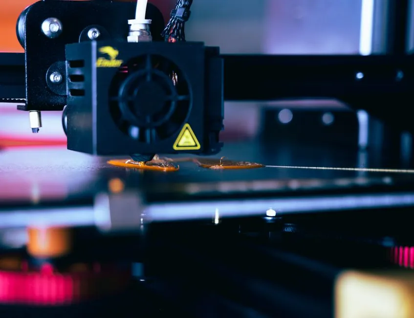
An AI accelerator in 2026 is built by chaining at least nine equipment stations, lithography, etch, deposition, CMP, inspection, metrology, ion implant, dicing, and advanced packaging, each with its own process-of-record tolerance window and a per-tool price band that varies by four orders of magnitude [S3].
The binding constraints on the 2026 tool set are no longer raw transistor count but joint availability of immersion or EUV exposure tools, hybrid bonding pick-and-place, and an AI-assisted EDA flow that can search a "very large solution space" of chip-design targets before tape-out [S3]. For context on how wafer supply feeds these lines, the 300 mm silicon wafer supplier map covers the upstream substrate side of the same chain.
Lithography: wavelength defines the capex tier
Immersion 193 nm ArF scanners remain the workhorse for 7 nm-class logic and HBM DRAM, while sub-7 nm AI accelerator tiers, typically DUV-multi-patterned or EUV-fed, use EUV steppers with a 13.5 nm source [S3]. The 2026 process literature explicitly catalogues immersion-defect yield-loss modes such as micro-bridging, pattern-collapse, and immersion-specific residue as the primary engineering targets [S3].
Selection on this station is wavelength-driven: immersion ArF for greater-than-or-equal-to 7 nm logic and DRAM with mature multi-patterning, EUV (13.5 nm) for 5/4/3 nm AI accelerator tiers, and nanoimprint or direct-write reserved for photonics and research wafers [S3]. Line-edge roughness (LER) and aerial-image contrast at the resist side are the two quantifiable sign-off criteria for line-side process engineers [S3]. A single EUV scanner lists above USD 200 million, and a high-volume fab needs 30–80 of them, which is why leading-edge fabs run capex programmes of USD 20–40 billion per site [S4].
Etch, deposition, and CMP: the three stations that turn exposure into a device
Plasma etch is specified by selectivity ratio and etch-profile cross-section, both named as engineering parameters in the 2026 process reference, where "loading effect" is flagged as a yield limiter when a single chamber processes open-frame and dense-array wafers back-to-back [S3]. Atomic-layer deposition (ALD) and PECVD handle the high-κ and low-κ stacks, while chemical-mechanical planarization sets the depth-of-focus budget for the next layer [S3].
Shibaura Mechatronics markets equipment that covers the full front-end-to-back-end chain on this basis, including handling tooling for the sub-2 nm device handling problem [S3]. Inline metrology (OCD, CD-SEM, e-beam review) gates the line at every critical layer, and every percentage point of die-yield improvement on a 4 nm-class GPU reticle can shift gross margin by single-digit points [S4].
Inspection, metrology, and ion implant: catching the defect before it costs a wafer
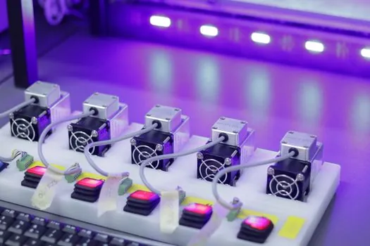
Integrated reticle inspection (IRIS) systems and post-etch defectivity tools are mandated at 5/4/3 nm because mask blank defectivity, not wafer yield, is the binding cost driver [S3]. The 2026 reference names "Integrated Reticle Inspection System (IRIS)" as a discrete tool category and treats it as a gating step between exposure and etch, with metrology at this layer being CD-SEM and optical critical-dimension (OCD) scatterometry with sub-nanometre repeatability [S3].
For ion implant, process engineers choose between high-current, medium-current, and plasma-doping (PLAD) tools, and the selection is doping-depth-driven: high-current for source/drain and well formation, medium-current for channel and lightly-doped-drain, and PLAD for fin or gate-all-around 3D structures where beam shadowing would otherwise cost yield [S3]. This station has no EUV-class peers, so the spec is more about dose uniformity (less-than-or-equal-to 0.5% across-wafer) than about absolute resolution [S3].
Advanced packaging: where the AI accelerator gets binned
Advanced packaging has displaced front-end lithography as the throughput bottleneck for AI accelerators; CoWoS, SoIC, and hybrid bonding are the three named 2026 packaging options, and they differ on interconnect pitch: CoWoS-RLL roughly 6 µm, SoIC-X roughly 3 µm, and direct Cu-Cu hybrid bonding below 1 µm [S3]. An H100-class accelerator pairs one GH100 GPU with six HBM3 stacks on a single interposer, while the SXM5 and PCIe Gen 5 form factors ship with five HBM stacks enabled and the H100 NVL ships with six, illustrating how the same silicon is binned into different SKUs after packaging [S4].
Package-level thermal design power routinely lands in the 700–1000 W band, which is why the final accelerator card uses vapor-chamber cold plates and specifies flow-meter-verified coolant loops [S4]. Throughput at this stage is gated by interposer area, TSV yield, and the availability of CoWoS-S/CoWoS-L lines, a known 2024–2026 supply bottleneck [S4]. On the equipment side, IC-Link by imec packages advanced packaging, testing, and quality assurance as an integrated line offering for accelerator makers [S3].
Edge-deployed AI accelerator hardware: spec ranges for industrial nodes
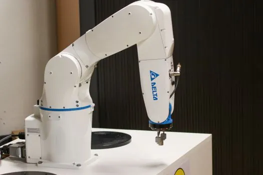
When AI inference runs at the industrial edge rather than in a data centre, the equipment specification collapses from EUV-class fab tools to a single industrial-grade accelerator card. Reference ranges for an industrial-edge GPU accelerator sit at FP32 peak 10–100 TFLOPS, board power 75–300 W, memory 8–48 GB HBM2e or GDDR6, and memory bandwidth 200–2000 GB/s over a PCIe 4.0 x16 host link [S2]. Environmental limits must be matched to the installation: operating temperature 0–70 °C, storage -40–85 °C, relative humidity 5–95% non-condensing, and ingress protection IP40–IP50 per IEC 60529 [S2].
Axelera AI's Metis AIPU targets exactly this industrial-edge slot, advertising up to 214 TOPS at sub-15 W typical board power with a fanless industrial thermal envelope for machine-vision, OCR, and 3D-pick applications [S1]. Reliability is benchmarked at MTBF 50,000–100,000 hours at 25 °C ambient, and physical integration fits a 267×112×40 mm, 0.5–1.5 kg card slot, which is the form factor machine builders design their chassis around [S2]. The trade-off versus a data-centre GPU is straightforward: you give up 2–3 orders of magnitude of FP32 throughput and you gain a fanless, lower-TDP card that can sit on a linear guide-driven vision stage or a crossed-roller guide-driven pick-and-place gantry inside a factory cabinet [S1][S2].
Selection criteria: who this guide is for, and who it is not for
This equipment map is for process-engineering and capex-planning teams at OSATs, foundries, advanced-packaging houses, and accelerator-system integrators who need a station-level bill of materials before a 2026–2027 fab or packaging-line decision [S3][S4]. It is not for buyers of off-the-shelf inference cards for PLC or SCADA retrofit work; those buyers should reference the industrial-edge accelerator spec ranges in the prior section instead [S1][S2].
Capability comparison across the named options, on a per-tool basis: EUV (13.5 nm) wins on resolution and is mandatory at 5/4/3 nm but loses on capex per tool and on aggregate tool count [S3][S4]. Immersion ArF is the lowest-risk workhorse for 7 nm-class and HBM DRAM but requires multi-patterning to reach the pitches an AI accelerator needs [S3]. CoWoS-RLL (6 µm pitch) is the volume-proven 2.5D choice for current H100-class parts, while SoIC-X (3 µm) and sub-1 µm Cu-Cu hybrid bonding are the named 2026 paths to higher HBM stack counts and tighter logic-memory pitch [S3][S4].
Standards, sourcing, and procurement references
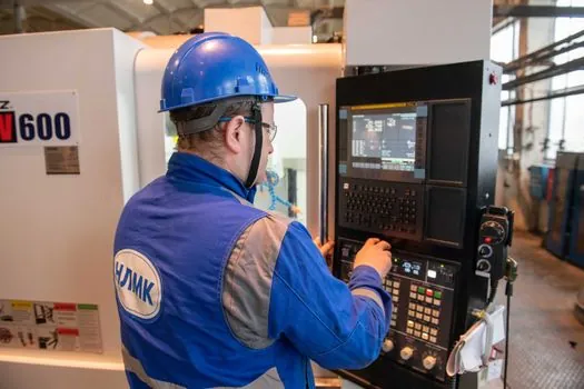
Compliance references for an industrial-edge accelerator procurement document include PCIe Base Spec 4.0 for the host interface and IEC 60529 for the IP40–IP50 ingress rating on a factory-floor card [S2]. On the fab side, the binding process standards are wavelength-defined (EUV at 13.5 nm source) rather than a single named spec, and the line-side sign-off is on line-edge roughness and aerial-image contrast at the resist side [S3]. Lead-time signals to track in the next two quarters are CoWoS-S/CoWoS-L tool deliveries (the named 2024–2026 bottleneck) and EUV scanner slot allocations, both of which gate accelerator volume more than any front-end yield programme [S3][S4].
For the relevant spec sheets and selection criteria, see additive manufacturing material.