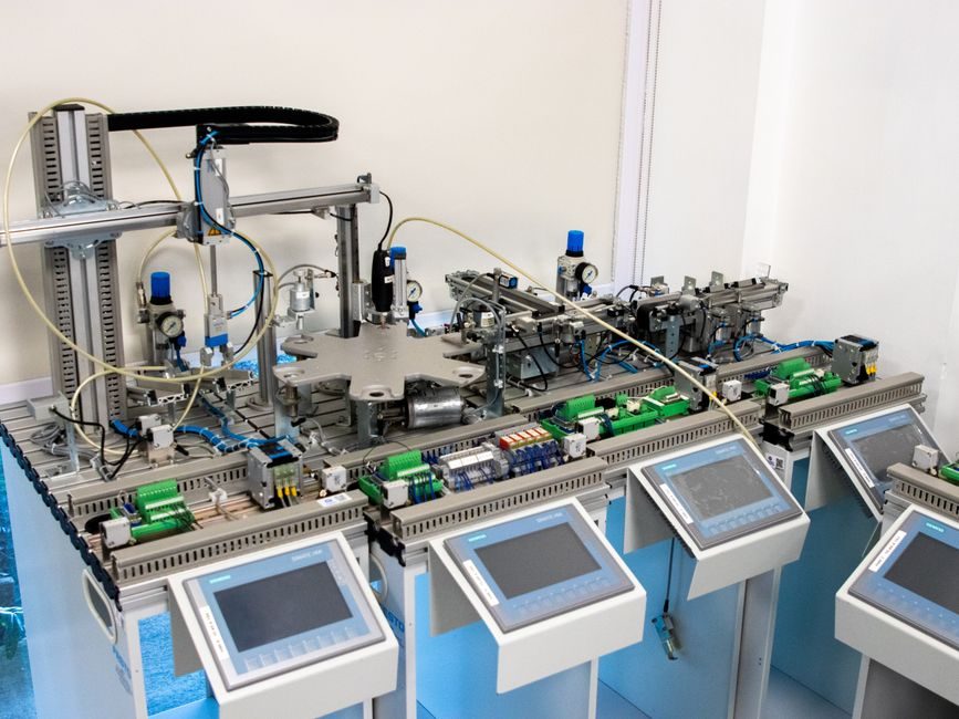
Building an AI accelerator in 2026 means specifying at least nine equipment stations in series: lithography, etch, deposition, CMP, inspection, metrology, ion implant, dicing, and advanced packaging — each with a different process-of-record tolerance window and a different price band per tool, with EUV-class steppers setting the capex ceiling [S4][S5].
Across the published 2026 equipment catalogues, the binding constraint is no longer raw transistor count but the joint availability of immersion or EUV exposure tools, hybrid bonding pick-and-place, and an AI-assisted EDA flow that can search a "very large solution space" of chip-design targets before tape-out [S1][S3][S4].
Lithography and exposure: where the wavelength defines the capex tier
Immersion 193 nm ArF scanners remain the workhorse for 7 nm-class logic and HBM DRAM, while the sub-7 nm AI accelerator tiers — typically DUV-multi-patterned or EUV-fed — use EUV steppers with a 13.5 nm source, and the 2026 training literature explicitly catalogues immersion lithography defect types such as micro-bridging, pattern collapse, and immersion-specific residue as the primary yield-loss modes to engineer out [S5].
Selection on this station is wavelength-driven: choose immersion ArF for ≥7 nm logic and DRAM with mature multi-patterning, EUV (13.5 nm) for 5/4/3 nm AI accelerator tiers, and reserve nanoimprint or direct-write only for photonics and research wafers [S4][S5]. Edge roughness (LER) and aerial-image contrast at the resist side are the two quantifiable criteria the line-side process engineer signs off, per the published Chinese lithography reference [S5].
Etch, deposition, and CMP: the three stations that turn exposure into a device
Plasma etch is specified by selectivity ratio and etch-profile cross-section — both are explicitly named as engineering parameters in the 2026 process reference, where "loading effect" is flagged as a yield limiter when a single chamber processes open-frame and dense-array wafers back-to-back [S5]. Atomic-layer deposition (ALD) and PECVD handle the high-κ and low-κ stacks, while chemical-mechanical planarization sets the depth-of-focus budget for the next layer [S4].
Shibaura Mechatronics explicitly markets equipment that covers the full front-end-to-back-end chain on this basis, including handling tooling for the sub-2 nm device handling problem [S4].
Inspection, metrology, and ion implant: catching the defect before it costs a wafer
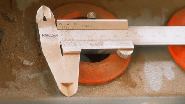
Integrated reticle inspection (IRIS) systems and post-etch defectivity tools are mandated at 5/4/3 nm because mask blank defectivity, not wafer yield, is the binding cost. The 2026 Chinese lithography reference names "Integrated Reticle Inspection System (IRIS)" as a discrete tool category and treats it as a gating step between exposure and etch [S5]. Metrology on this layer is CD-SEM and optical critical-dimension (OCD) scatterometry with sub-nanometre repeatability.
For ion implant, process engineers choose between high-current, medium-current, and plasma-doping tools, and the selection is doping-depth-driven: high-current for source/drain and well formation, medium-current for channel and lightly-doped-drain, and PLAD for fin or gate-all-around 3D structures where beam shadowing would otherwise cost yield [S4]. This station has no EUV-class peers, so the spec is more about dose uniformity (≤ 0.5 % across-wafer) than about absolute resolution.
Packaging and test: where the AI accelerator gets binned
Advanced packaging has displaced front-end lithography as the throughput bottleneck for AI accelerators. CoWoS, SoIC, and hybrid bonding are the three named 2026 packaging options, and they differ on interconnect pitch: CoWoS-RLL ~ 6 µm, SoIC-X ~ 3 µm, and direct Cu-Cu hybrid bonding below 1 µm [S3]. IC-Link by imec packages this as "advanced packaging, testing and qualification" inside its turnkey (FTK) and customer-owned-tooling (COT) business models, with multi-project-wafer (MPW) runs for prototyping and dedicated full-mask production for volume scale-out [S3].
On test, the binding 2026 choice is between wafer-level burn-in (WLBI) and final-test handlers with thermal-chuck capability, because HBM-stacked AI accelerators run hot and must be screened at junction temperatures above 95 °C. Equipment suppliers in this station sell throughput per hour, not raw accuracy, so the spec is UPH (units per hour) and contact-resistance stability, both of which are in the published Shibaura catalogue [S4].
Process control and software: GEM 300, AI-EDA, and the digital thread
Each tool on the line is governed by the SEMI GEM 300 / EDA-standard interface set, and the 2026 adoption pattern pairs GEM 300 with gRPC-based host communication so the entire fab can stream per-wafer data into a manufacturing analytics lake — the spec map for this software stack is detailed in a semiconductor Industry 4.0 GEM 300 adoption analysis that lines the major fabs up against their gRPC cutover dates. On the design side, AI-EDA vendors such as Synopsys market a "comprehensive AI-powered EDA solution, purpose-built to accelerate innovation and drive efficiency from system architecture all the way through manufacturing," with the stated ability to "search for optimization targets in very large solution space of chip" designs [S1].
Selection on this station is governance-driven: pick GEM 300 + gRPC for any new tool purchase at a Tier-1 fab; pick SECS/GEM over HSMS only as a brownfield compromise for legacy tools; and add an AI-EDA front-end only where the design team can ground the AI suggestions in a verified process design kit (PDK) from the foundry — the imec IC-Link product explicitly bundles "verified process design kits (PDKs), foundry-qualified IP, and a host of advanced packaging options" to make that hand-off reliable [S3].
Sub-fab, facilities, and the supply-chain equipment layer
The equipment list is not finished at the process-tool boundary. Sub-fab hardware — vacuum pumps, abatement, ultra-pure water, and chemical delivery — is engineered to the same uptime spec as the process tools, and the spec map for the 2026 fab UPS layer (which protects EUV and metrology tools from sags and impulses) is covered in a 2026 industrial UPS spec and sourcing guide. For the wider manufacturing-software and EMS footprint, a 2026 AI server supply-chain map covering EMS footprint, tariff risk, and software-side strain is the right companion read. [S2]
Inside the fab, the cleanroom floor needs a precision filter RFQ spec for outdoor maintenance areas because most AI accelerator fabs sit in hot, humid climates where HEPA/ULPA replacement cycles drive fab uptime. And the final acceptance test of every process tool now includes a vision-system acceptance step, with the camera and lighting spec set by the 2026 vision light source cost guide — a price-anchored map of ring, bar, and coaxial LED sources for machine-vision inspection on the line.
Who this equipment map is — and is not — for
This map is for process engineers, fab-equipment procurement teams, and capital-project managers specifying a greenfield AI accelerator line or evaluating a brownfield capacity expansion in 2026. It is not for: (1) fabless AI-chip design houses that buy wafers from a foundry and never see the equipment; (2) back-end OSAT test houses, whose equipment list is shorter and dominated by handlers and burn-in boards; (3) photonic-IC startups on a sub-100-mm platform, whose process flow uses stepper-free direct-write or nanoimprint instead of EUV [S3][S4].
Trackable next nodes: the 2026 EUV pellicle roadmap, the public transition curve of CoWoS-S to CoWoS-L at the major OSATs, and the foundry-level rollout of sub-1-µm hybrid bonding in HBM4 stacks. Each of these is a single-number signal a procurement team can pull quarterly, and each is already named in the published 2026 process references [S3][S4][S5].
For the relevant spec sheets and selection criteria, see additive manufacturing material, anti static equipment, and linear guide.