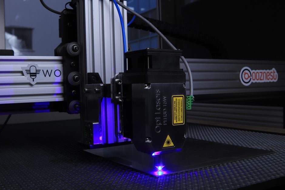
An AI accelerator is produced through three sequential manufacturing stages — chip design, wafer fabrication, and advanced packaging — before the bare die is mounted on a PCB, surrounded by HBM stacks, and racked as a data-center accelerator [S3].
According to an analysis by Epoch AI, an estimated 40% of the growth in training compute has been due to using larger numbers of chips, with the remainder split between using higher-performance AI chips (~27%) and training models for longer durations (~33%) [S3].
Design Stage: From Microarchitecture to GDSII Layout
Design begins with high-level workload targets — inference latency, training throughput, TOPS/W — that designers translate into a microarchitecture, a logic model, and finally a physical GDSII layout using electronic design automation (EDA) software [S3].
Logic blocks are either built in-house or licensed as IP cores from third-party vendors, then stitched into a multi-billion-transistor floorplan; the resulting AI ASIC or GPU is functionally verified, timing-closed, and signed off for tape-out before any silicon is produced [S3]. For context on how EDA and tape-out fit into a wider smart-factory stack, the lithography smart-manufacturing line map breaks down the tool classes that consume those layouts. Because this is the cheapest stage to fix a mistake, design verification typically absorbs the largest share of engineering hours in the whole AI chip program.
Fabrication Stage: Photolithography, Etch, and Deposition on 300 mm Wafers
Fabrication converts the GDSII layout into physical transistors by repeating four basic unit operations — lithography, etch, deposition, and chemical-mechanical polishing — across a 300 mm silicon wafer through dozens of mask layers [S3].
Leading AI parts target sub-5 nm process nodes using EUV lithography, where each exposure step directly drives wafer cost; a single EUV scanner lists above USD 200 million, and a high-volume fab needs 30–80 of them, which is why leading-edge fabs now run capex programmes of USD 20–40 billion per site [S3]. Yield at this stage is the dominant cost lever — every percentage point of die-yield improvement on a 4 nm-class GPU reticle can shift gross margin by single-digit points, and inline metrology (OCD, CD-SEM, e-beam review) gates the line at every critical layer. Process engineers measure line health with the same kind of inline sensing stack described for TOPCon cell process control, only at orders of magnitude tighter tolerances. Compared with the back-end-of-line automation mapped in the DRAM smart-manufacturing back-end map, the FEOL/MEOL flow here is more chemistry-intensive and less conveyor-dominated.
Packaging Stage: CoWoS, HBM Stacking, and 2.5D Integration
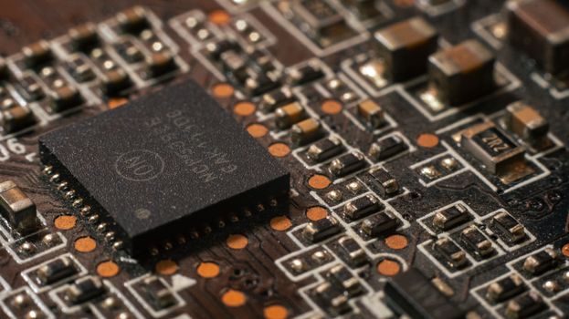
After singulation, the AI die is recombined with high-bandwidth memory and I/O chiplets using 2.5D or 3D packaging — most commonly Chip-on-Wafer-on-Substrate (CoWoS) with silicon interposers — because HBM stacks and the logic die must share a tight physical pitch to sustain multi-TB/s memory bandwidth [S3].
An H100-class accelerator pairs one GH100 GPU with six HBM3 stacks on a single interposer; the SXM5 and PCIe Gen 5 form factors ship with five HBM stacks enabled, while the H100 NVL ships with six, illustrating how the same silicon is binned into different SKUs after packaging [S3]. Throughput at this stage is gated by interposer area, TSV yield, and the availability of CoWoS-S/CoWoS-L lines — a known 2024–2026 supply bottleneck. Package-level thermal design power routinely lands in the 700–1000 W band, which is why the final accelerator card uses vapor-chamber cold plates and specifies a flow-meter-verified coolant feed and a pressure transmitter-monitored cooling loop. The principles of inline inspection at this stage mirror the separator inline-vision stack, adapted to AOI of microbumps and underfill fillet geometry.
AI Accelerator Types and Their Manufacturing Trade-Offs
The dominant AI accelerator categories — GPUs, TPUs, FPGAs, ASICs, neuromorphic chips, and edge AI accelerators — differ in design intent, not in fab process: all six are produced on essentially the same CMOS tooling, but their mask count, IP mix, and packaging choice shift dramatically [S2].
Across the four decision criteria that matter to a process engineer — performance per watt, time-to-silicon, unit cost at volume, and flexibility post-tape-out — the types line up as follows: GPUs (e.g., NVIDIA H100) sit at high performance/W and high unit cost with low flexibility, but win on time-to-silicon because they reuse a stable microarchitecture across generations; TPUs are full-custom ASICs with the highest performance/W at volume but years of design lead time; FPGAs offer full post-silicon reconfigurability at the cost of 5–10× lower peak TOPS/W; and edge AI accelerators trade peak throughput for sub-10 W envelopes and bare-die-plus-fan packaging rather than CoWoS [S2]. Neuromorphic chips remain a research-grade category with low volume and no standard packaging. The additive manufacturing material choices for accelerator cold plates and the multifunction process calibrator work required to qualify those loops are part of the same factory commissioning envelope.
Use Cases, Limits, and Failure Modes in Volume Production
Volume AI accelerator manufacturing is gated by four limits: leading-edge wafer capacity (sub-5 nm EUV lines are concentrated at three foundries), CoWoS advanced-packaging capacity, HBM3/HBM3E supply, and the cooling infrastructure that lets a 700–1000 W package run sustained workloads [S3].
Typical field failure modes traced back to manufacturing include HBM stack solder-joint fatigue under thermal cycling, TIM pump-out between die and cold plate, and underfill voiding in CoWoS — all of which are screened by acoustic microscopy, X-ray CT, and burn-in at the back-end test step. Where a fab is being commissioned alongside a power-hungry data center, the industrial valve and process-control stack has to be qualified to the same audit standard as the wafer-tool gas panels, and the V-process line reference for vacuum-handling subsystems is a useful analogue for the vacuum and gas-delivery blocks in EUV scanners. Process engineers closing out a new accelerator line should track three verifiable signals: monthly HBM bit-shipment growth, CoWoS wafer-out per month per OSAT, and EUV tool uptime at the bottleneck scanner.