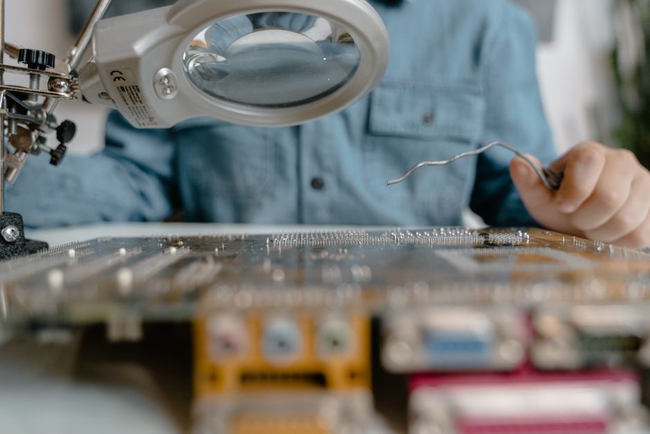
An AI accelerator's bill of materials is dominated by four line items — wafer fabrication at the leading node, 2.5D/3D advanced packaging, HBM stack, and large-area substrate — and every other cost (IP licensing, verification, test, masks) sits on top of that stack [S1].
The cost split shifts sharply with process node: a 3 nm wafer costs several multiples of a 7 nm wafer, and the advanced-packaging step that glues HBM to the logic die now rivals the wafer itself in dollar terms for high-end GPUs and training accelerators [S1].
Wafer fabrication: node, yield, and mask cost
Wafer cost is set by node, wafer size, and defect density, and is the single largest variable in an AI chip's cost stack; AnySilicon's semiconductor manufacturing cost breakdown lists wafer, packaging, test, and ASIC cost factors as the four primary buckets that engineers must size before quoting [S1]. Mask sets at N5/N3 run into the tens of millions of USD per full set, so non-recurring engineering (NRE) is amortised across a fixed production volume — break that volume and the per-die cost spikes because masks are paid regardless of yield.
Gross die per wafer falls as die area grows, so a 700 mm² accelerator die yields a fraction of the dies a 100 mm² mobile SoC yields from the same wafer; the 300 mm wafer baseline is standard for any AI-class logic, while 200 mm persists only for analog, MEMS, and power management on the same die [S1]. Yield curves on a new node typically ramp over 6–12 months, and a 10–20 percentage-point yield delta at the start of a production run is the difference between a profitable and a money-losing quarter for a fabless AI-chip house.
Advanced packaging: CoWoS, 2.5D interposer, and HBM integration
Packaging is the second cost pillar and, for AI accelerators that pair a large logic die with multiple HBM stacks, often the first: 2.5D CoWoS-S / CoWoS-L with silicon interposer is the dominant approach for HBM3/HBM3e/HBM4 attachment, and the interposer plus micro-bump assembly is a separate billable step from wafer fab [S1]. Thermal density on a CoWoS package can exceed 1 kW per package on a flagship GPU, so the integrated heat-spreader / cold-plate solution is part of the packaging cost envelope, not a free add-on.
2.5D capacity is the binding constraint on AI-chip shipments in 2026; a single CoWoS line is sized to a fixed number of interposers per month, and the line's allocation between NVIDIA, AMD, and the hyperscaler-internal ASICs is what determines the volume ceiling. Alternatives — fan-out wafer-level packaging (FOWLP) and 3D hybrid bonding — are in production for specific products but do not yet match CoWoS on HBM-channel count per package, and the hybrid-bonding tooling has a steeper per-wafer cost than thermocompression micro-bumping at this point.
HBM stack: HBM3e / HBM4, capacity per stack, and signal integrity
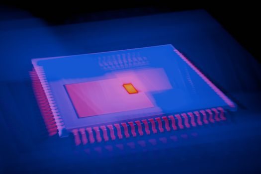
HBM is sold per stack, and each stack typically holds 8 or 12 dies with through-silicon-via (TSV) interconnects; HBM3e ships at 8–12 Hi stacks with 24 GB capacity per stack, while HBM4 expands the channel count and pushes per-stack capacity higher, and the per-GB price of HBM tracks DRAM commodity pricing with a premium for the TSV process and known-good-die test [S1]. An AI accelerator that uses 6–8 HBM stacks therefore carries a memory-subsystem cost that can rival the logic die itself in absolute dollars.
Selection between HBM3e and HBM4 is set by bandwidth target: HBM3e delivers roughly 800–900 GB/s per stack, HBM4 pushes the per-stack figure past 1 TB/s, and the system-level memory bandwidth drives how many stacks the package must hold, which feeds back into package size and interposer cost. If your model fits in 24 GB per stack with HBM3e, you stay on the cheaper, more available part; if you need 1 TB/s+ per package, the HBM4 cost premium is unavoidable and you budget for it at the architecture stage, not the procurement stage.
Substrate, PCB, and board-level integration
The large organic substrate that carries the CoWoS package is itself a constrained resource: an AI-grade substrate is typically a 6–8 layer build with very high layer-to-layer alignment tolerance, and the supply is concentrated in a small number of Taiwanese and Japanese vendors. Substrate lead time has been the schedule-binding item for multiple AI-server programs, and the per-unit substrate cost for a flagship accelerator is in the high-tens to low-hundreds of USD — material, versus the much larger packaging and HBM line items that surround it. [S1]
At the next assembly level, the AI accelerator lands on a server PCB that is almost always an HDI or high-layer-count build with controlled-impedance routing for PCIe Gen5/Gen6 and 400G/800G Ethernet; contract manufacturers quote these as part of an OEM/ODM package with factory-direct pricing and transparent cost breakdown, where volume discounts kick in at multi-thousand-unit batch size [S2]. For low-volume or prototype builds, the same fabricators offer fast-turn prototyping and turnkey assembly, which lets a startup burn down a design without committing to a full panel.
IP licensing, verification, and NRE amortisation
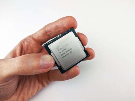
Pre-silicon cost is the smallest line on a per-die basis but the largest non-recurring engineering bucket: a modern AI accelerator integrates tens to hundreds of third-party IP blocks (DDR/LPDDR controllers, PCIe, CXL, SerDes, on-chip interconnect / NoC, security, and DSP), each carrying per-use or royalty fees. AnySilicon's IP-vendor taxonomy is built around exactly these blocks — memory and PHY IP, CPU and peripherals, analog and mixed-signal, interface controllers, and wireline/wireless communication IP — and the licensing stack is one of the four primary cost factors the breakdown flags [S1].
Verification, DFT, and test development also sit in the NRE bucket and are non-trivial at AI scale: an accelerator with a large die, multiple HBM PHYs, and a coherent fabric needs a verification environment in the multi-million-USD range before tape-out, and that cost is paid once per project, not per die. For a fabless AI-chip company, the rule of thumb is that NRE plus masks plus one round of respin is the minimum capital call before a part can ship in volume, and any spec change after tape-out moves that number sharply.
Test, yield, and reliability cost overlay
Test cost has two pieces: wafer sort (probe) and final test, plus the burn-in / reliability screens that are standard for any high-ASP AI part. Wafer-probe cost scales with probe-touch count and the number of HBM PHYs that must be exercised per die, and final-test time on the package is dominated by the at-speed SerDes and HBM training sequences — minutes per unit on a flagship part is not unusual. [S1]
Known-good-die (KGD) testing of HBM stacks before integration is its own line item, and a single bad HBM die can scrap the whole packaged unit; that is why HBM vendors price in a yield margin and why the cost stack above already includes a KGD overhead in the per-GB price. Reliability screens at the package level — thermal cycling, HTSL, HTOL — are mandatory for any accelerator going into hyperscaler datacenters, and the screen cost per unit is small in dollars but real in cycle time and floor space.
Total cost of ownership and sourcing signals
Purchase price is roughly half the AI-chip total cost of ownership story; the other half is yield, scrap, and field failure. A 5–10% in-line yield loss at advanced packaging is industry-typical for a new CoWoS product, and a 1% field failure rate on a $30k accelerator sold to a hyperscaler is a warranty exposure larger than the margin on many OEM/ODM assembly contracts. [S1]
Trackable signals to watch: capacity allocation across CoWoS lines, HBM3e-to-HBM4 mix in shipping accelerators, substrate lead time, and any public mask-set or respin announcements from the major AI-chip vendors. For buyers outside the hyperscaler tier, AI Chip Capacity Planning: Wafer, Substrate, and AI-Planner Stack maps how those allocations translate into delivery dates, and AI chip manufacturing equipment: a 2026 spec-driven buyer's map walks the tool side of the same supply curve.
For the relevant spec sheets and selection criteria, see additive manufacturing material, pressure transmitter, and flow meter.