
Pairing electroluminescence (EL) imaging with conventional visual inspection is the only practical way to screen silicon PV modules for both cosmetic damage and the sub-surface defects (micro-cracks, broken gridlines, inactive cell regions) that drive long-term power loss [S1][S2]. End-of-line factory tests typically run EL, IV flash, and Hi-pot on every module, while third-party pre-shipment inspection (PSI) re-runs the same gates to catch handling damage introduced after the manufacturer's own quality checkpoint [S2].
Production-line throughput drives the inspection architecture: wafer handling runs above 3,000 cells/hour, cell printing inspection above 2,000 cells/hour, and stringer tolerances for silver contact placement sit inside 50 microns, so any inline defect that escapes these stations becomes a yield and warranty liability [S3]. For a useful overview of the manufacturing process and the lamps and light fittings used in dark-box EL rigs, see the encyclopedia entry.
Defect Taxonomy: What Visual Inspection Catches and What It Misses
Visual inspection covers frame damage, glass scratches, delamination bubbles, junction box misalignment, backsheet cracking, EVA browning/whitening, burn marks on junction boxes, and corroded mounting hardware; these are surface phenomena an inspector can see and document with photographs [S4]. The same walk-through verifies grounding terminations, mounting torque, and thermal-expansion spacing, since electrical safety and mechanical integrity ride on those bolted joints [S4].
Visual inspection cannot resolve micro-cracks inside silicon, sub-spec Pmax, broken or missing silver fingers, encapsulant voids smaller than the bubble-detection threshold, or shunted cell regions. A 45-degree crack running from a gridline and a 5 W shortfall on a 400 W module both look identical to the eye on a pallet, and that is the failure mode that makes EL and IV flash testing non-optional for serious pre-shipment work [S1].
EL Imaging: Principle, Camera Choice, and Field Conditions
EL imaging works by forward-biasing the PV cell so the semiconductor emits near-infrared light, the same electroluminescence effect that makes an LED glow, then capturing that emission with a high-resolution CCD or InGaAs camera inside a darkened enclosure or at night in the field [S2][S5].
Sinovoltaics' on-site methodology recommends nighttime imaging so that production is not interrupted, and Intertek CEA runs the same night-shift approach for what it describes as the world's largest nighttime EL test, surveying hundreds of thousands of modules with investor- and insurance-grade image resolution [S2][S5]. The same cameras and dark-box hardware are now integrated into inline post-lamination stations where 100% module screening is the target rather than sampling [S3].
IV Flash Test Acceptance Criteria and STC Tolerance
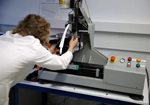
Flash testing at Standard Test Conditions (irradiance 1000 W/m², cell temperature 25 °C, AM1.5G spectrum) compares each sampled module's Pmax, Voc, and Isc against the manufacturer's datasheet, with the commonly applied PSI tolerance band of +3%/-0% on Pmax (modules may over-perform but must not under-perform by more than 3%) [S1].
Factory flash tester calibration drift, batch-to-batch cell binning variation, and selective reporting of flash data are documented sources of Pmax shortfalls that a third-party flash re-run is specifically designed to expose, making IV verification the electrical-performance companion to the structural-integrity data from EL [S1]. Hi-pot (dielectric withstand) testing typically runs in the same end-of-line sequence, since insulation breakdown is a safety-class failure that IV and EL alone cannot flag [S2].
Inline vs Pre-Shipment Inspection: Where the Gates Sit
Manufacturer end-of-line gates run at every station from wafer through final module: pre-print wafer inspection at 3,000+ wafers/hour, cell printing at 2,000+ cells/hour, post-diffusion colour and edge-isolation check, stringing (ribbon placement, solder joint quality, post-handling crack detection), post-lamination EL with 100% module screening, and final visual on appearance, labelling, junction box, and frame [S3].
Pre-shipment inspection sits downstream of palletization and re-checks both gates because handling damage (compression stacking, rough container loading) can crack cells that passed factory EL, and that is damage the manufacturer would not have seen on its own line [S1]. A reference workflow starts with visual to triage obviously broken modules, then runs EL and IV on the survivors, since feeding a broken module into an EL rig wastes test time and can confuse the resulting image interpretation [S1]. For context on how inline camera stations compare with end-of-line lighting equipment and electric lamps used in dark-box EL rigs, see the encyclopedia entry.
AI-Assisted Visual Inspection Throughput and Edge Architecture

AI visual inspection is positioned as quality infrastructure for gigawatt-scale cell and module lines, with coverage at wafer, cell, stringer, lamination, and final module stages, classifying defect type and severity automatically rather than relying on human reviewers for every image [S3].
Edge-AI architecture is the deployment model most cited for solar factories: inspection data is processed in real time on the line without cloud connectivity, which matters for production-data confidentiality and for plants in regions with limited network infrastructure [S3]. On the AI side, deep-learning models are trained on cell-crack morphologies (edge cracks, diagonal cracks, finger interruptions), printing defects (missing fingers, broken busbars, silver-paste smearing, misregistration), wafer defects (chips, pinholes, contamination, colour variation), and diffusion defects (edge isolation failures, shunts) [S3]. At module level the same models flag post-lamination cell cracks, encapsulant voids and bubbles, delamination, cell misalignment, ribbon misalignment, soldering defects, frame sealing failure, and junction-box placement and adhesion defects [S3].
Micro-Crack Severity and the Inspection-Economics Argument
Micro-cracks are present in most commercial PV installations, so the engineering decision is not whether to accept any cracks but where to draw the severity line and how to enforce it [S1][S5]. A severe micro-crack can propagate under thermal cycling, deactivate cell area, and trigger bypass-diode activation or hot-spotting, all of which are safety-class events, not just yield-loss events [S5].
Catching severe cracks at the factory gate is cheaper than discovering them in the field: logistics for replacement modules, crane time, and lost energy yield all stack up after shipment, while a third-party EL pass during pre-shipment inspection runs in a fixed time window and gives the buyer a documented baseline to attach to a warranty or workmanship claim if a dispute arises later [S1][S5]. EL image libraries from factory QA work also feed into root-cause analysis when a field failure does occur, since the comparison between as-shipped and as-installed images shows whether the damage originated in production or in handling [S5].
Standards Anchor and Decision Boundaries
IEC 61215 is the design-qualification and type-approval reference cited for crystalline-silicon PV modules, and Solar Power Europe's best-practice guidance, built on the EU Horizon 2020 SolarBankability studies, recommends IEC 62446 plus additional in-situ EL imaging as the inspection baseline for operating plants [S2][S3]. Pass/fail criteria on the EL image itself are not a single fixed threshold; they depend on crack type and quantity per cell or module, and qualified third parties maintain internal criteria libraries that buyers can request and compare against the manufacturer's own pass standards [S2].
Decision rule of thumb: if a buyer's only inspection step is visual, accept the cosmetic risk and the documentation gap; if IV flash is added, accept that sub-surface cell defects are still invisible; only the EL + visual + IV combination closes the structural-integrity, electrical-performance, and safety-insulation gates in one pass. See also how linear module inline test stations differ from dark-box EL rigs in the encyclopedia, and how relay-driven station hand-off compares with camera-gated hand-off in the relay module entry.
Trackable next signals: (1) whether buyer-side PSI providers publish their 2026 EL crack-morphology libraries against the IEC 61215 / IEC 62446 update cycle, and (2) whether AI-vision suppliers expand from cell-level to stringer-level inline coverage at the documented 3,000 cells/hour wafer-station throughput [S3].
See also our earlier report, ASTM A1035 Grade 100 vs Grade 120: Spec, Strength, and Selection.