
HBM (High Bandwidth Memory) is a 3D-stacked DRAM family that uses through-silicon vias (TSV) to bond multiple DRAM dies on a silicon interposer beside the host compute die, multiplying bandwidth while reducing power per bit versus conventional DDR [S4]. The JEDEC standard JESD238B.01, published April 2025, formalises HBM3 with a wide-interface architecture and independent 64-bit channels, where channels are not necessarily synchronous to each other [S2].
The 2026 HBM market is shaped by AI accelerator demand, ongoing JEDEC standard evolution, and the first credible mobile HBM roadmap for smartphones in 2026 and beyond [S1][S3]. Leadingir's 2026 global and China HBM industry report maps the segment across stacked DRAM supply, near-memory computing integration, and the PNM / PIM / CIM architecture split [S1].
JEDEC JESD238B.01: the HBM3 interface and channel model
JEDEC's JESD238B.01 (HBM3 DRAM, published April 2025) is the controlling standard for the HBM3 generation that the industry is shipping into AI accelerators in 2026 [S2]. The standard is hosted in JEDEC's Main Memory committee track, alongside DDR SDRAM, with the interface defined in the JC-42 (Solid State Memories) family [S2].
The defining architectural points published in the standard are: the HBM3 DRAM is tightly coupled to the host compute die through a distributed interface, the interface is divided into independent channels, each channel is completely independent of the others, channels are not necessarily synchronous, and each channel interface maintains a 64-bit data bus operating at double data rate [S2]. That independent-channel, wide-interface model is the reason HBM3 can deliver hundreds of GB/s of aggregate bandwidth to a single GPU or AI ASIC package.
Why HBM: bandwidth, power, and the 3D-stacked DRAM advantage
HBM was created to solve two specific problems in modern DRAM: it substantially increases bandwidth available to computing devices such as GPUs, and it reduces power consumption per transferred bit [S4]. The mechanism is 3D stacking with TSV, then mounting the stack on the same interposer as the compute die, which both saves die area and shortens the data path [S3].
The second-generation HBM (HBM2) was the first JEDEC-published revision to address the capacity and clock-rate limits of the original HBM spec, raising both stack height and per-pin data rate versus the first generation [S4]. From HBM2 onward the design intent has been the same: a wide, parallel, short-reach interface that pushes more bits per watt than a discrete DDR channel can deliver to a distant DIMM [S2][S4].
Near-memory, in-memory, and in-storage compute: the 2026 architecture split

Per the 2026 Leadingir HBM industry report, the broader compute-near-storage landscape is split by physical distance between storage and compute cells: Processing Near Memory (PNM), Processing In Memory (PIM), and Computing in Memory (CIM) [S1]. HBM is the substrate that makes PNM economically attractive, because the memory and the compute die already sit on the same interposer and the bandwidth is high enough that data movement stops being the bottleneck.
The PNM tier integrates memory and compute cells through chip packaging and board-level assembly to increase memory-access bandwidth and reduce data movement, raising overall compute efficiency [S1]. PIM and CIM push logic further into the DRAM array itself; in 2026 these remain more experimental than PNM, but they share the same upstream driver: AI workloads are starving for memory bandwidth, and stacking the DRAM next to the logic die is the cheapest way to feed it [S1][S2].
Mobile HBM: Apple, Samsung VCS, SK hynix VFO, and the 2026+ roadmap
Mobile HBM is the newest branch of the HBM family and the one with the most volatile 2026 supply picture. Apple is reported to be in talks with both Samsung Electronics and SK hynix to bring HBM into the iPhone line for a 20th-anniversary model, with on-device large-model AI cited as the driver [S3]. Samsung is developing a package approach called VCS, while SK hynix is using VFO, and both vendors target mass production in 2026 or later [S3].
Three engineering constraints keep mobile HBM from being a straight transplant of data-centre HBM. First, manufacturing cost is far higher than incumbent LPDDR, which has to be absorbed somewhere in the BoM [S3]. Second, an iPhone is a thin-and-light thermal envelope, and a 3D-stacked DRAM on the same interposer as the SoC adds a serious heat-density problem [S3]. Third, the TSV and 3D-stacking process is highly complex, so yield is the gating metric for whether mobile HBM hits the cost target that a smartphone BoM requires [S3]. For buyers tracking the segment, the watch items are vendor mass-production timing, package technology choice (VCS vs VFO), and the first phone SKU that ships in volume [S3].
Selection logic: HBM vs LPDDR vs DDR in 2026 system design
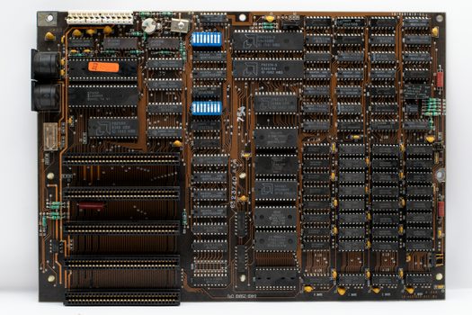
Three criteria decide which memory a 2026 design team picks: bandwidth per watt, board area, and BoM cost. HBM wins on bandwidth per watt and on area (because the stack and the compute die share one interposer), and loses on cost and supply diversity [S3][S4]. LPDDR is the low-power DDR branch, sitting in a separate JEDEC track, and remains the default for phones and thin laptops where HBM's cost and thermal load are unacceptable [S2][S3]. Conventional DDR SDRAM remains the lowest-cost per bit and the broadest supply base, so it stays the right call for capacity-bound workloads that are not bandwidth-bound [S2].
For an AI accelerator card, HBM3 (per JESD238B.01) is the right pick: the 64-bit independent channels and wide-interface architecture are exactly what large-matrix-multiply workloads need [S2]. For a smartphone SoC, the trade-off still favours LPDDR in 2026, with mobile HBM gated on package yield, cost, and thermal solution maturity [S3]. For a general server or edge node without an AI workload, DDR remains the cost-optimised choice [S2].
Where to track HBM supply and demand signals through 2026
Two indicators tell you whether the 2026 HBM cycle is loosening or tightening. The first is stack height and per-stack capacity on JEDEC-compliant HBM3 parts from the three major suppliers; the second is the volume timing of mobile HBM SKUs, because that is the next demand pool after AI accelerators and the one that will most affect 2026 wafer allocation [S1][S3]. Engineers selecting a pressure transmitter for an AI server coolant loop or a flow meter for a fab water system can ignore the memory market; engineers selecting a PLC for an OSAT tool should not, because HBM supply tightness has historically rippled into back-end packaging capacity that competes for the same OSAT lines.
Background reading: Plastic Pipe Buying Guide 2026: Resin, Pressure, and Cost Tiers.