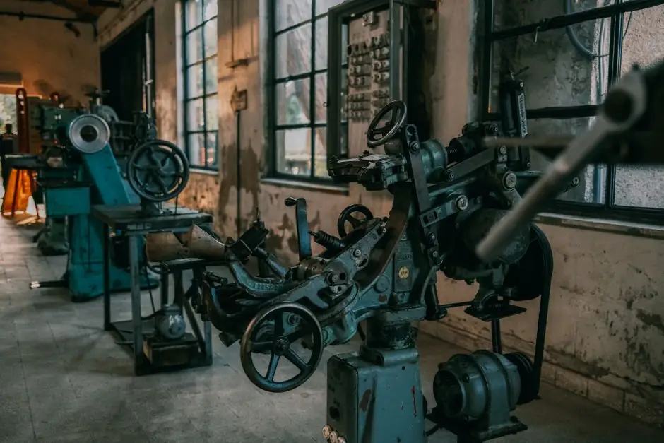
Lithography tool pricing spans roughly two orders of magnitude, from sub-$15M I-line steppers used in mature fabs to EUV scanners priced at $120M-$200M each, with total system market value pegged at $30.4B in 2026 [S2][S4][S5].
Behind those headline prices sit five cost drivers: light-source technology, stage and optics precision, cleanroom-grade mechanical isolation, software/computational lithography stack, and ongoing service contracts that materially affect lifetime cost. The same year-over-year ratio holds whether you are buying a 1991 stepper or a 2025 High-NA EUV: capital equipment, labor, and facilities dominate the per-good-die cost equation [S1].
Price Tiers by Scanner Class
The cheapest production-class systems, I-line steppers, sell for $5M-$15M per unit and handle mature nodes at 365 nm wavelength, with Canon shipping units such as the FPA-5550iX (50x50 mm field, 0.5 micrometer resolution) into sensor and micro-OLED lines [S3][S5]. KrF scanners (248 nm) sit in the $20M-$40M band, used for non-critical layers and memory [S5].
ArF immersion systems (193 nm wavelength, water-immersed optics) range from roughly $40M-$60M per unit and remain the workhorse for 7 nm-class multi-patterning layers, even in fabs that also run EUV [S4][S5]. EUV (13.5 nm) scanners are the top of the pricing stack at $120M-$200M, and High-NA EUV pushes beyond that [S4]. On a per-wafer-cost basis the early EUV debate was settled by total cost of ownership: throughput, yield, and process-step reduction offset the acquisition premium versus multi-patterned DUV [S4].
What Drives the Cost: Five Engineering Buckets
1) Light source. Excimer lasers for KrF/ArF and the tin-droplet laser-produced plasma (LPP) source for EUV dominate optical-engine cost. EUV source power scaling from early 60-80 wafers-per-hour class tools toward 150-200 wph is the single biggest lever on per-wafer cost [S4]. 2) Projection optics. Mirrors for EUV are multi-layer Mo/Si-coated aspheres figured to sub-angstrom surface errors, and contamination control (pellicles, hydrogen ambient) adds recurring cost [S4]. 3) Stage metrology. Nanometer-class overlay requires interferometer-stabilized air-bearing stages and is a major fraction of mechanical cost across every tier [S1].
4) Computational lithography and software. Inverse lithography, OPC, and ML-driven source-mask optimization are now integral cost items, both in tool capex and in fab operating cost [S4]. 5) Service, installation, and facilities.
Lithography vs Total Fab Capex: Where the Money Goes

That share is heavily weighted toward the leading edge: TSMC alone allocated a large fraction of its $38B 2025 capex to lithography for 2 nm fabs in Hsinchu and Kaohsiung; Intel's Ohio One campus is sized for more than 20 EUV scanners at full ramp [S5]. The market is also concentrating geographically: Asia Pacific held 58.7% of lithography equipment revenue in 2025, with pure-play foundries contributing nearly 60% of end-user spend [S2][S5].
That concentration means fabs in Taiwan, South Korea, and the mainland consume the bulk of new EUV and ArF immersion capacity, while new government-backed capacity in the US, EU, Japan, and India reshapes the demand map through 2030 [S2][S5]. For sourcing teams mapping construction-machinery-and-equipment needs alongside fab build-outs, the implication is that lithography cell build-out often competes for the same specialized HVAC, vibration-isolation, and cleanroom sub-trade capacity.
Total Cost of Ownership: Acquisition Is the First Number, Not the Last
The 1991 IEEE/SEMI long-term cost-of-ownership model identified stepper throughput, overlay, yield, utilization, process automation, and upgrade path as the parameters that actually move cost-per-good-die, with capital cost being only one of them [S1]. That conclusion still applies: a $150M EUV tool that runs 150 wph at 90% utilization with high yield beats a cheaper system burdened by multi-patterning steps, even before service and energy costs.
Energy and consumables add another layer. EUV's tin-fuel, hydrogen, and pulsed-power consumption, plus pellicle replacement, drive a measurable opex delta versus DUV, which the industry is closing through source-power scaling and uptime improvements [S4]. For fab planners modeling 10-year TCO, the practical pattern is: purchase price sets the headline, throughput x yield sets the wafer-cost outcome, and service plus energy closes the gap between the two. The same spec-first logic used in pneumatic-actuator TCO modeling applies to scanner selection: drive decisions off lifetime cost per wafer, not sticker price.
Selection Criteria: Who Needs Which Class
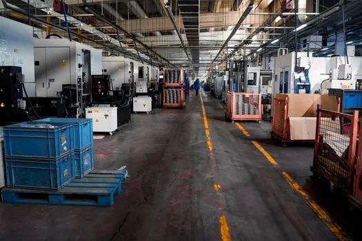
First-line criterion is minimum feature size. I-line and KrF cover geometries above ~110-130 nm; ArF immersion covers down to 7 nm with multi-patterning; EUV is mandatory for sub-7 nm single-exposure layers and is being adopted in DRAM for active patterning [S2][S5]. Second criterion is wafer volume: EUV is justified only at high-volume leading-edge fabs, where throughput and per-wafer cost displace the acquisition premium.
Third is upgrade path. The IEEE/SEMI model concluded that flexible, upgradeable, high-throughput steppers running simultaneously at full spec deliver the lowest per-good-die cost, a logic that modern fabs extend to EUV-to-High-NA upgrade agreements [S1]. Fourth is supplier concentration: ASML holds near-monopoly control over EUV systems, while I-line, KrF, and ArF immersion have a broader supplier base including Canon and Nikon, which materially affects negotiation leverage and lead time [S5]. For diversified industrial buyers, similar concentration dynamics affect how explosion-proof electrical and specialty-equipment tenders are scoped.
Limitations, Failure Modes, and Sourcing Risks
Supply risk: with one supplier dominating EUV, lead time and service-contract terms are the de facto constraint on fab ramp schedules; DUV classes offer shorter lead times and multi-source competition [S5]. Process risk: EUV pellicle defects, mask-blank defects, and source-power instability directly translate into wafer-cost excursions; the industry is investing in pellicle robustness and source uptime as primary cost-reduction levers [S4].
Spec risk: datasheet wph ratings are nominal, and real throughput depends on overlay rework, exposure field count per wafer, and maintenance windows; a 200 wph rating can deliver 150 wph effective in production [S4]. Cost-modeling risk: per-good-die economics are sensitive to yield assumptions, and the 1991 IEEE/SEMI work warned that mismatched overlay or utilization assumptions invalidate cost comparisons between tools [S1].
Standards and Reference Anchors
Lithography equipment sits under the IEC 60079-series for any subsystems used in flammable atmospheres, ISO 14644 for cleanroom classification, and SEMI standards (E10, E12, E48, E78 families) for equipment reliability, automation, and interface definitions that govern how steppers and scanners are specified and accepted at customer sites [S3]. For cost modeling, the IEEE/SEMI long-term cost-of-ownership methodology remains the reference framework for ranking parameters that move per-good-die cost [S1].
For fab engineering teams cross-spec'ing adjacent capital equipment, the same cleanroom and reliability framework governs lighting-equipment-and-electric-lamps and anti-static-equipment selection, where particulate and ESD control budgets are written against the same ISO 14644 and SEMI E78 envelopes that frame lithography tool specs.
Trackable signals through 2026: EUV TAM trajectory toward roughly $10B by 2026 at 21.5% CAGR per public market analysis [S4], the High-NA EUV ramp at Intel's Ohio One and TSMC's 2 nm lines [S5], and the Asia Pacific share of lithography spend holding above 55% as new US/EU/Japan fabs come online [S2]. For procurement teams, those three signals are the cleanest read on whether 2026 EUV lead times are lengthening or easing, and whether DUV supply remains the flexible margin in any tool-mix decision.