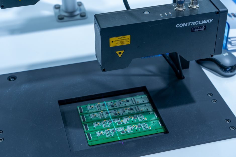
Selecting PCB manufacturing equipment is a process-engineering decision driven by layer count, substrate family, and annual throughput rather than brand prestige; a 4-layer FR-4 prototype line and a 28-layer rigid-flex line require fundamentally different imaging, etching, and inspection stations [S1][S6].
Process-engineering buyers as of August 2026 should treat the equipment list as a configurable toolchain — laser direct imaging (LDI), photochemical etching, electroless and electrolytic plating, and automated optical inspection (AOI) each represent a distinct cost and capability node, with single-station pricing in 2026 commonly running from roughly US$5,000 for a small photochemical etching machine to over US$1 million for a fully automated LDI+AOI line [S4].
Equipment Categories That Define a PCB Fabrication Line
A modern PCB fab line is built from six functional station groups: pre-production engineering (CAM), imaging, etching and developing, plating, mechanical finishing, and inspection; Fastlink's published capability matrix, which lists Rigid, Flex, Rigid-Flex, Hybrid RF/Digital, Metal Core, and Aluminum-Backed PCB offerings, illustrates how each substrate family pulls a different combination of stations from that pool [S3]. PCBWay's own process disclosure — Customer-supplied Gerber data feeding into PPE (Pre-Production Engineering) before imaging — confirms that CAM software and front-end tooling are the first line items, not an afterthought [S6].
Substrate family drives the most consequential choices: a Metal Core or Aluminum-Backed line requires plating baths and etching chemistries tuned for high thermal-conductivity cores, while a Hybrid RF/Digital line needs LDI capable of resolving fine-pitch features alongside controlled-impedance test stations [S3]. Shenzhen Wonderful Technology (WDFPCB), operating since 1996, advertises a 1-to-28 layer capability with turnkey assembly, which is only achievable when the equipment pool supports both fine-line imaging for high-layer-count work and high-throughput conveyorised lines for volume 4- to 8-layer FR-4 [S2].
Selection Criteria: Volume, Layer Count, and Substrate Family
The first decision axis is volume profile: quick-turn prototype shops, where individual jobs may complete in hours rather than days, lean heavily on direct imaging, in-line AOI, and small-footprint wet benches to compress changeover time [S1]. PCBWay's published positioning as a prototype and small-batch supplier to designers, R&D departments, niche-market electronics firms, universities, and research establishments maps directly to that equipment profile [S6].
The second axis is layer count and stack-up complexity: a 28-layer rigid-flex build with controlled impedance needs laser drilling, sequential lamination presses, and via-fill plating capability, while a 4-layer double-sided FR-4 panel can be served by a single LDI exposure and a conveyorised DES (develop-etch-strip) line [S2][S6]. The third axis is substrate thermal and RF behaviour — metal-core LED boards and Rogers high-frequency laminates both need process-specific chemistries and cannot share plating baths with standard FR-4 [S3].
For buyers mapping the decision, four criteria are worth scoring explicitly: (1) minimum line/space resolution the imaging station can hold, typically 50–75 µm for LDI versus 100 µm+ for conventional phototool exposure; (2) substrate family coverage (FR-4, flex polyimide, metal core, RF laminates); (3) layer-count ceiling (1–28 layers is now common in mid-tier Asian fabs); and (4) inspection depth — 2D AOI only versus 2D + 3D solder-paste and final-etch AOI [S1][S3][S6].
Key Equipment Types and 2026 Cost Bands
Laser Direct Imaging (LDI) replaces film phototools by writing the artwork directly onto photoresist, eliminating registration error between layers; this is the single most capital-intensive station in a new line and the most common bottleneck for shops upgrading from 100 µm to 50 µm features [S1]. Photochemical etching machines — typically stainless-steel spray-etch tanks rated for cupric chloride or ferric chloride chemistries — are entry-level capital equipment; a Beijing-based OEM lists a stainless-steel photo chemical etching machine at roughly US$5,500 per set with a 1-set minimum order, representative of small-scale entry pricing in 2026 [S4].
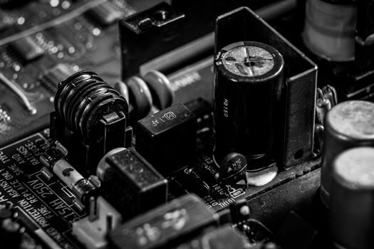
Plating lines split into electroless copper (for through-hole and blind-via metallisation), electrolytic copper (for build-up and pattern plating), and surface-finish lines (ENIG, ENEPIG, HASL, OSP, immersion tin/silver); ENIG chemistry is increasingly specified for fine-pitch and wire-bond work, while HASL remains the cost default for through-hole and higher-volume consumer work [S3]. PCB cleaning equipment, including in-line and batch stencil/substrate cleaners, is sold as a distinct station on Alibaba's industrial-machinery listings in 2026, with pricing typically in the US$3,000–US$40,000 band depending on conveyor width and ultrasonic load capacity [S5].
Who Quick-Turn Equipment Is For — and Who Should Avoid It
Quick-turn PCB manufacturing, defined as jobs completing in hours rather than the days-to-weeks of a traditional queue, is engineered for design-iteration cycles, prototype validation, and low-volume niche-market builds where time-to-market outweighs unit cost [S1]. It is a poor fit for high-volume consumer runs where per-panel pricing dominates the business case and dedicated hard-tooled lines beat a flexible quick-turn cell on cost per square metre [S1][S6].
Buyers evaluating quick-turn capacity should also weigh five specific benefits documented by the source material: significant manufacturing-cost savings from early defect detection, avoided defects through prototype-stage correction, saved delivery time via manufacturability reviews, reduced mid-production change orders, and the chance to incorporate client feedback before tooling commits — all of which are direct consequences of having CAM, LDI, and AOI co-located rather than split across vendors [S1]. For higher-volume applications, the same equipment set configured for 24/7 conveyorised flow delivers a different cost-per-panel profile and is not directly comparable to a quick-turn cell on first principles [S6].
Process Flow and Where Each Station Sits
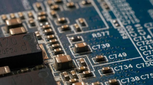
PCBWay's published 11-step process — PPE, cutting, inner-layer imaging, inner-layer etching, inner-layer AOI, lay-up and lamination, drilling, through-hole plating, outer-layer imaging and plating, solder-mask application, surface finish, routing, and final test — is representative of how 2026 fabs sequence the equipment [S6]. Inner-layer imaging and inner-layer AOI are the two stations where defect-cost is lowest; catching a short or open at this stage avoids scrapping an already-laminated multilayer board, which is why LDI + inner-layer AOI is the single highest-ROI upgrade path for a 4- to 8-layer FR-4 shop [S6].
For flex and rigid-flex lines, the additional steps are coverlay cutting and bonding, flexible material handling with dedicated vacuum chucks, and laser skiving for partial-depth cavities; these are not optional add-ons, and shops that route flex panels through a rigid-only line will see yield losses that no amount of upstream AOI can recover [S3]. The same logic applies to metal-core and aluminium-backed boards, where the thick dielectric and copper balance demands different drilling parameters and dedicated contour-routing tooling to avoid delamination at the metal interface [S3].
Quality Systems, Sourcing Models, and Standards to Verify
Quality control in 2026 PCB fabs is documented at three levels: incoming substrate inspection, in-process AOI, and final electrical test; the source material consistently references "PCB assembly inspection equipment" and "components quality control equipment" as discrete line items alongside the manufacturing stations themselves, which is the minimum kit a turnkey shop needs to claim one-stop service [S2]. Shenzhen Wonderful Technology (WDFPCB), in operation since 1996 and serving more than 100 countries, exemplifies the turnkey model — layout, design, fabrication from 1 to 28 layers, assembly, and component sourcing are all delivered from a single facility, and the equipment list has to support each handoff [S2].
Buyers comparing suppliers should map each candidate's published capability list against four verifiable claims: (1) substrate families actually offered (Rigid, Flex, Rigid-Flex, Hybrid RF/Digital, Metal Core, Aluminum-Backed per Fastlink's disclosure); (2) layer-count ceiling and minimum line/space; (3) surface-finish options in-house (ENIG, HASL, OSP, immersion tin/silver); and (4) inspection stack (2D AOI, 3D AOI, flying-probe, bed-of-nails, impedance coupon test) [S2][S3]. Lead time is a fifth axis: quick-turn lines are now routinely measured in hours for prototype quantities, but volume runs still require days-to-weeks and that gap is structural, not a vendor failure [S1].
Limits, Failure Modes, and Trackable Signals
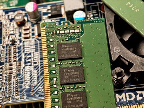
The most common failure mode in a 2026 PCB fab is registration drift between layers in a multilayer build, which is what LDI was designed to solve; the second is under- or over-etching in the DES line, which is what in-line chemistry control and AOI cross-checks are designed to catch; the third is plating voids in through-holes, addressed by electroless copper bath chemistry control and via-fill plating where blind/buried vias are present [S1][S6]. Each of these is a station-level failure, not a process-level one, and the equipment selection directly determines whether the failure is caught at inner-layer AOI (cheap) or after lamination (expensive) [S6].
Trackable signals for 2026 procurement: confirm the supplier's stated layer-count ceiling against actual panel samples at that layer count; verify which surface finishes are run in-house versus outsourced to a sub-contract plater; ask for AOI defect Pareto data, not just an AOI station count; and cross-check whether quick-turn advertised lead times apply to the build configuration being quoted, since lead times for 28-layer rigid-flex are not the same as those for 4-layer FR-4 [S2][S3][S6]. The pressure transmitter reference architecture, where sensing technology and signal protocol must match the process medium, is a useful analogy — PCB stations are not interchangeable, and pairing the wrong imaging or plating tool with a substrate family produces scrap rather than boards. For shops scaling up, the flow meter spec philosophy applies: define the measurable operating envelope first, then size the equipment to it, rather than letting vendor brochures drive the spec.
For the relevant spec sheets and selection criteria, see additive manufacturing material.
For related coverage, see Silicon Wafer Industry 4.0 Adoption: Specs, Standards, and Fab Floor Reality in 2026.