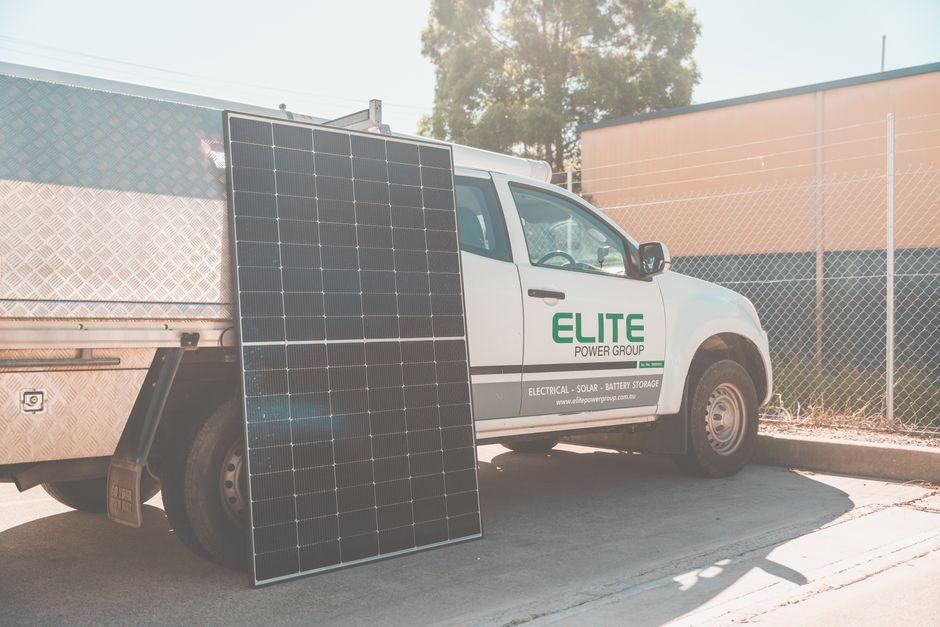
PV raw-material sourcing is dominated by four input families — metallurgical- and monosilicon feedstock, mono- or multicrystalline wafers, front- and rear-side silver paste, and EVA/POE encapsulant plus backsheet — and 2026 procurement specs are written around those four lines, not around finished-module brands [S1].
The cost stack of a c-Si module still tracks silicon content: polysilicon (USD/kg), wafer (USD/pc), cell (USD/W) and laminate (USD/m²) — three of which are quoted in different units, which is why buyers must normalise everything to USD/W before comparing suppliers. Minority-carrier lifetime, the parameter Ames Laboratory and the two-photon microscopy work both flag as the single most variable PV-materials figure, is set at the wafer and cell step, so procurement discipline upstream pays for itself downstream [S2][S3].
Polysilicon Grades and the Mono/Multi Split
Polysilicon for PV is sorted into metallurgical-grade (MG-Si, ~98–99% purity), solar-grade (SoG-Si, 6N–7N) and electronic-grade (9N+), with c-Si PV cells consuming solar-grade as the dominant feedstock; mono wafer lines effectively require 7N+ material because impurity-driven lifetime loss directly caps cell Voc, the open-circuit voltage that two-photon carrier-lifetime mapping is designed to characterise non-destructively [S2].
Spec discipline at this tier means fixing the resistivity band (typically 1–3 Ω·cm for p-type mono Czochralski), the oxygen and carbon target (≤10 ppma each for high-lifetime wafers), and the format — chunk, rod or granular — before any price talk. Granular polysilicon feeds fluidised-bed reactor (FBR) mono lines and avoids the crushing step that chunk material requires, which is why Siemens-process chunk still dominates butcher-bar mono lines and granular dominates FBR [S1].
Wafer Format, Thickness and Diamond-Wire Tolerances
The 2026 wafer field is a duopoly of M6 (166 mm) legacy stock, M10 (182 mm) mainstream volume and G12 (210 mm) large-format mono, with p-type PERC gradually yielding market to n-type TOPCon and HJT; diamond-wire sawing is the universal cutting method, with wire diameter down to 55–65 µm and wafer thickness centred on 150 µm for M10 and 160 µm for G12, trending toward 130 µm and 140 µm respectively as kerf-loss economics tighten. [S1]
Procurement specs at the wafer step should pin diameter tolerance (±0.25 mm), thickness tolerance (±10 µm), TTV (total thickness variation, ≤5 µm for premium mono) and bow/warp (≤50 µm) — those four numbers, written into the PO, are what separate a Tier-1 wafer from a usable-but-suspect lot. Lifetime is fixed here: a 150 µm M10 mono PERC wafer from a controlled cooling run will routinely show bulk minority-carrier lifetime above 1 ms, while a poorly gettered multicrystalline wafer lands at 30–100 µs, which is the practical spread buyers are paying for [S2].
Silver Paste Load and the Copper-Print Question
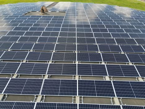
Front-side silver paste consumption on a PERC cell sits in the 80–120 mg/cell range and the rear-side at 100–150 mg/cell, giving a combined 180–270 mg/cell silver load that translates to roughly 10–15 g per 100 W of module output; n-type TOPCon drives the upper bound because both sides are silver-printed (bifacial, no aluminium BSF), so a G12 TOPCon cell lands closer to 250–350 mg/cell combined. [S2]
Like steel section suppliers where chemistry and profile band jointly drive the price, silver reduction is a chemistry + process question, not a sticker-price question.
Encapsulant, Backsheet and Front Glass
EVA (ethylene-vinyl acetate) remains the default encapsulant at 0.45–0.50 mm sheet weight around 350–400 g/m², but POE (polyolefin elastomer) has become the default for n-type TOPCon and HJT where PID (potential-induced degradation) resistance and lower moisture-vapour transmission matter more than raw cost. Backsheet choices split into KPK (PVDF/PET/PVDF, 25-year weatherability), TPT (Tedlar/PET/Tedlar, legacy 25-year) and transparent backsheet for bifacial — each with a peel-strength target ≥40 N/cm at the EVA interface. [S3]
Front glass has converged on 3.2 mm semi-tempered low-iron with anti-reflective coating for utility-scale and 2.0 mm for rooftop; spec the iron content (<150 ppm Fe₂O₃), the AR coating (MgF₂ or porous-SiO₂, gain target 2–3% absolute) and the mechanical load rating (5400 Pa snow, 2400 Pa wind are the typical IEC 61215 test points buyers replicate in incoming inspection). EVA moisture uptake above 0.5 wt% correlates with acetic-acid-driven corrosion of cell metallisation, so incoming-lot moisture spec at <0.1 wt% is non-negotiable on long-life contracts.
Comparison of the Four Main Cell Architectures on Sourcing Criteria
[S4]
The procurement signal in that table is that polysilicon grade, silver-paste chemistry and encapsulant choice co-determine efficiency — there is no single silver-bullet spec, and chasing the highest-efficiency number without locking the supporting inputs produces field-failure risk that buyers absorb in O&M cost, not in BoM savings. Copper-paste and copper-plating technology shares the same 'chemistry + process' interaction buyers see in hydraulic accumulator sourcing, where pre-charge gas, bladder material and port type all have to be specified together.
Failure Modes Buyers Should Spec Against
The five failure modes a 2026 incoming-inspection regime should test for are: PID (potential-induced degradation, recoverable by grounding or by POE encapsulant choice); LeTID (light- and elevated-temperature-induced degradation, primarily a PERC concern above 75 °C); snail trails (encapsulant- and silver-paste-driven, screened by 1000 h DH at 85 °C/85% RH); cell cracking (controlled by wafer TTV and stringer handling, screened by EL imaging at ≥0.5 mm/s line speed); and backsheet delamination (peel-strength drop after 2000 h UV, screened by ASTM D903 or equivalent). [S1]
For perovskite-silicon tandems the additional raw-material risk is the perovskite-precursor chemistry — PbI₂, FAI, MAI and the lead-encapsulation strategy — which is why tandem sourcing today is closer to a chemicals-supply contract than a wafer-supply contract; the Ames Laboratory Rashba-effect work and the two-photon carrier-lifetime microscopy technique are both directly applicable to perovskite-film metrology, not just c-Si [S3][S2].
Standards and Reference Documents for Incoming Inspection

The standards a PV raw-material buyer should reference on every PO are: IEC 61215-1:2021 (design qualification for c-Si modules), IEC 61730-1/-2 (safety qualification), IEC 62804-1 (PID test method), UL 61730 (North American safety), and IEC 61215-1-4 for bifacial — plus ASTM E903 for encapsulant transmittance and ASTM D903 for backsheet peel strength; these are the documents auditors will ask for, not the standard a sales rep names on a slide. [S2]
The most useful tracked signals for 2026-07 are: polysilicon spot price (USD/kg) and the mono/multi wafer premium, the TOPCon/HJT production-share split at the cell step, and the silver-paste mg/cell figure on the latest Tier-1 BOM disclosures — those three numbers, updated monthly, are the leading indicators of where module ASP (average selling price, USD/W) will land 6–9 months out. Buyers who treat the BOM as a single number, rather than as the four-line breakdown above, will be the last to know when one input — silver, polysilicon, EVA, or G12 wafer — moves against them. For the broader materials context, the quartz material properties reference covers the high-purity quartz supply chain that feeds silicon-metal production.
For component-level specifications, see linear guide, and crossed roller guide.