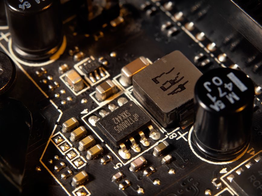
A 2026-spec power semiconductor fab line couples Class 1 / ISO 14644-1 cleanroom bays with sub-micron wafer inspection, laser-assisted die attach, and end-of-line electrical test for IGBT, MOSFET, SiC MOSFET, and GaN HEMT devices [S1][S2]. Discrete power components in scope cover FETs, MOSFETs, IGBT singles/modules, Zener/bridge rectifiers, TVS diodes, SCR/TRIAC thyristors, JFETs, and power driver modules [S1].
The line is engineered for two parallel pressures: shrinking SiC and GaN feature sizes that push inspection below 1 µm, and rising currents/voltages per package (650 V–1700 V SiC MOSFET, 100 V–650 V GaN) that drive thermal management and burn-in test throughput [S5].
Cleanroom, Utility, and Wafer-Flow Layout
A greenfield power-device fab typically sequences incoming silicon/SiC wafer inspection, epitaxy or implant, diffusion/oxidation, lithography, etch, CMP, metallization, anneal, backside grind, and wafer-level test before dicing and packaging [S2]. Each metrology node — wafer prober, defect review, optical critical dimension — sits inside a Class 1000 to Class 100 (ISO 14644-1) bay, with bumping and laser-assisted bonding typically located at ISO Class 7 or better to control particle adders [S4].
Power semiconductor lines differ from logic fabs in two structural ways: die-per-wafer is much lower (typical 150 mm and 200 mm SiC wafers are common, with 300 mm SiC in qualification), so wafer-handling automation is sized for heavier, thicker substrates; and backside metallization (Ti/Ni/Ag stacks for SiC diodes and MOSFETs) demands a dedicated spatter-controlled area before dicing [S5].
Utilities — high-purity DI water, bulk N<sub>2</sub>, clean dry air (CDA), process vacuum, and RF/DC sputter power — are sized by the sputtering tool count, not the lithography count, because power-device fabs are typically metal-heavy (3–5 metal layers versus 10+ in advanced logic). For comparison context, the cost line items inside this scope mirror those broken out in Power Semiconductor Manufacturing Cost: Wafer, Packaging, Test Breakdown.
Vision Inspection and Metrology Stack
Basler's semiconductor product range is a useful baseline for what a 2026 vision stack looks like: CXP-12 and 5GigE area-scan cameras, racer 2 TDI line-scan cameras, ace 2 X SWIR / X UV variants, and 3D options including ToF and stereo cameras are deployed from wafer processing through final packaging [S2]. CXP-12 is the dominant interface for high-throughput die-level AOI, with 5GigE used on slower inspection islands where cabling reach matters more than raw bandwidth.
Lighting choices follow the defect type: bar lights and flat dome lights dominate wafer backside and lead-frame inspection; coaxial and dome lights handle mirror-finish die-top measurements; SWIR cameras target silicon and SiC subsurface defects (typical SiC is opaque in visible but partly transmissive past ~1.1 µm); UV variants support resist and polyimide imaging [S2]. The expected defect-detection target is sub-µm for sub-3 µm nodes and low-single-digit µm for mature 5 V–40 V MOSFET lines.
Frame grabbers (imaFlex 2, imaWorx, microEnable 5 marathon) and trigger boards synchronize multi-camera inspection cells to the conveyor or track indexer; trigger latency is the throughput bottleneck, not pixel rate, in most power-device AOI deployments [S2].
Laser Process Modules Inside the Line
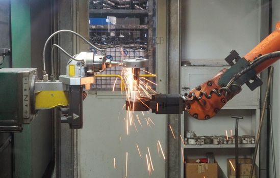
Diode laser beam sources have been common in semiconductor production since the 1990s, originally for marking and labeling, and have expanded into laser-assisted bonding of complex components such as flip chips, wafer prober illumination for optoelectrical inspection, and selective soldering of high-mass lead frames [S4]. For power-device packaging specifically, laser-assisted soldering is the preferred process for the heavy Cu clip and ribbon terminations on SiC MOSFET modules where reflow profiles risk voiding.
Wavelength selection is driven by the substrate absorption curve: blue (around 450 nm) and near-IR (around 800–940 nm) diode-laser stacks are standard for Cu and Al soldering, with kW-class fiber-coupled diode sources used for selective sintering of Ag-sinter die attach in high-reliability SiC modules [S4]. The same laser class is used for wafer-scribing and dicing of SiC, which is mechanically hard and requires either laser stealth dicing or ablation-assisted cleaving.
Discrete Power-Component Family and Test Coverage
The end-of-line test plan must cover every discrete family the line ships: power MOSFETs (single, RF, and arrays), IGBTs in single, hybrid, and module packages, rectifier bridges, TVS diodes, MOV varistors, SCRs, TRIACs, DIACs/SIDACs, JFETs, and pre-biased BJT arrays [S1]. Each family has a distinct test vector: MOSFETs need gate-charge (Qg), R<sub>DS(on)</sub> at multiple V<sub>GS</sub>, and avalanche energy (E<sub>AS</sub>); IGBTs add short-circuit withstand time (t<sub>sc</sub>) and V<sub>CE(sat)</sub> vs temperature; TVS and MOV require high-current pulse verification (typically 8/20 µs or 10/1000 µs waveforms).
Component-package testing extends into the protection-device portfolio — PTC resettable fuses, GDT gas discharge arresters, inrush current limiters (ICL), thermal cutoffs, and TVS thyristors — each defined by a different surge profile that the ATE must source [S1]. This is where the 2026 spec map begins to converge with broader Industry 4.0 / smart-factory work; see Power Semiconductor Industry 4.0 Adoption: SiC/GaN Fab Stack and 2026 Spec Map for how MES integration, predictive maintenance, and digital-twin yield models layer on top of this physical test floor.
Failure Analysis and Reliability Lab
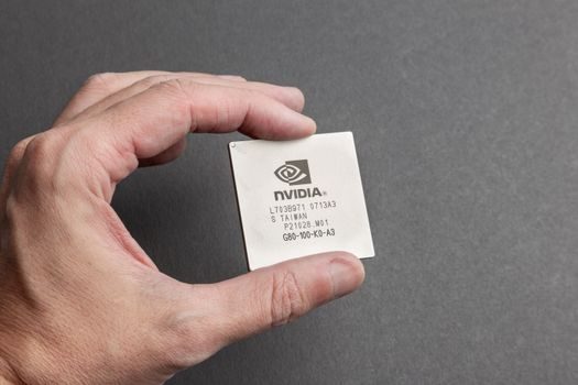
Thermo Fisher's power-device FA workflow is a realistic template: large-area cross-section sample prep (mechanical + ion-beam polishing), SEM/TEM fault localization, and electrical characterization including dynamic R<sub>DS(on)</sub> vs temperature and thermal impedance Z<sub>th</sub> sweeps [S5]. Large-area cross-sectioning of power modules — typically 10 mm × 20 mm packaged IGBT or SiC MOSFET modules — is the single hardest sample-prep step and a common reason FA cycle time runs 2–4 weeks.
Sample-prep tools and SEM/FIB capacity are the capacity bottleneck for any new line aiming at automotive-grade reliability; AQG-324-qualified suppliers run a permanent FA lab, not a shared one, because cycle time directly gates customer PPAP [S5].
Selection Criteria and Line-Type Comparison
Four dominant line archetypes compete in 2026: mature 200 mm silicon MOSFET/IGBT lines, 150 mm SiC MOSFET lines, 200 mm GaN-on-Si HEMT lines, and 300 mm SiC qualification lines. On four decision criteria — capex per wafer-out, cleanroom burden, inspection capital intensity, and time-to-1 kW-module qualification — the comparison is concrete enough to spec against. [S2]
1) Capex per wafer-out: 200 mm Si MOSFET is the cheapest baseline, 150 mm SiC roughly 1.6–2× that figure, 200 mm GaN-on-Si roughly 1.3–1.5×, and 300 mm SiC (in qualification) is the highest at 3× or more, dominated by the cost of the ion implanter and SiC-specific CMP tools. 2) Cleanroom burden: SiC and GaN lines are less lithography-driven and so tolerate ISO Class 5 in some bays where Si logic would demand Class 3, but die-attach and bonding islands still hit ISO Class 7. 3) Inspection capital intensity: SiC's micropipe and basal-plane dislocation densities make SWIR and photoluminescence-based inspection mandatory, adding ~10–15% to the vision budget versus a Si line. 4) Time-to-qualification: Si MOSFET is shortest, GaN-on-Si intermediate (driven by GaN-specific reliability models), SiC MOSFET the longest (driven by AQG-324 and HV-H3TRB requirements).
For a line builder weighing the options, the decision narrows fast: if the product mix is below 200 V and consumer, stay on 200 mm Si MOSFET; if the product is 650 V–1700 V automotive or traction, SiC is unavoidable; if the product is 100 V–650 V high-frequency datacom or fast-charging, GaN-on-Si is the better fit.
Limitations, Constraints, and Failure Modes

The two hard constraints on any 2026 power-device line are SiC wafer supply (150 mm and 200 mm are supply-constrained, with 300 mm still pre-production) and qualified process tooling for high-temperature ion implantation above 500 °C [S5]. Without both, the line cannot meet automotive AEC-Q101 and AQG-324 gates. Inspection capital is the second constraint: SWIR and UV cameras, plus high-NA objectives, are not off-the-shelf for SiC thickness, and delivery lead times routinely run 6–9 months for built-to-order microscope systems [S2].
Common failure modes in newly commissioned lines are well known: voiding under Cu clip bonds in SiC modules (laser-assisted soldering with closed-loop pyrometry is the current mitigation), gate-oxide degradation from inadequate charge control during test, and HTRB / HV-H3TRB escapes that are usually root-caused to test-board leakage paths, not the device. Each of these is a line-design decision (process tool, handler socket, test-board layout), not a downstream quality decision.
Trackable next signals: whether 200 mm SiC wafer volume scales to relieve the supply pin (capacity expansions at the two leading suppliers are the leading indicator), and whether 300 mm SiC shifts from R&D to pilot — either of which would re-rank the cost ratios above. The AQG-324 / AEC-Q101 audit calendar for the next two automotive model years will set the demand baseline for new fab capacity in parallel.
For component-level specifications, see molding line, automatic molding line, and conveyor sorting line.