SEMI's published manufacturing-process overview defines the modern fab as a two-part operation: front-end-of-line (FEOL) transistor build, and back-end-of-line (BEOL) interconnect, plus a separate back-end-of-fab (assembly, packaging, test) that turns finished wafers into packaged devices [S1]. The front-end alone combines ten or more unit process steps — thermal oxidation, photolithography, plasma etch, ion implant, diffusion, chemical-mechanical planarization, thin-film deposition (CVD/PECVD/ALD, PVD), wet clean, inspection, and metrology — repeated in layers, typically 50-100 mask levels for a leading-edge logic part [S3].
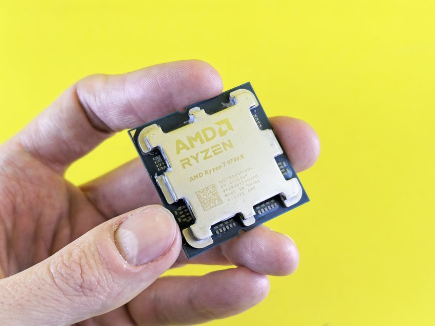
Intel's 18A and 14A process pages list a stack that adds gate-all-around (GAA / RibbonFET) architecture, backside power delivery (PowerVia) and sub-nm-class EUV patterning to the conventional flow [S2]. Across all nodes, the 300 mm fab line is structured around cleanroom ISO Class 3-5 zones, a 75-100 kW/m² tool heat-load envelope, and ultra-pure water (UPW) demand of roughly 4-10 m³ per wafer pass — the figures the SEMI PFAS explainer uses to anchor the environmental footprint discussion [S1].
Front-End Unit Processes: Ten Step Families, Real Temperature Windows
Thermal oxidation of silicon at 800-1200 °C in dry O₂ or steam grows a SiO₂ gate/isolation dielectric; rapid thermal processing (RTP/RTO) at 1000-1100 °C for 1-30 s handles thin anneal oxynitrides [S3]. Photolithography at advanced nodes uses 193 nm immersion ArF scanners (NA 0.33) stepping down to 13.5 nm EUV (NA 0.33, rising to 0.55 high-NA), with line/space pitches already at 18 nm in single-pattern EUV layers and 12-14 nm targeted with double patterning [S2].
Plasma etch — ICP, CCP, cryogenic — runs at 10-100 mTorr with RF bias of hundreds of watts, selectivity 5:1 to 50:1 versus the hard mask and 20:1 to 100:1 versus SiO₂; chemistry is typically halogen-bearing (Cl₂, BCl₃, HBr, SF₆, CF₄/C₄F₈) for silicon and fluorocarbon-bearing for oxide [S3]. Ion implant energies span 0.2 keV (for sub-1 nm junction formation) to multi-MeV for well doping; thermal anneal is now dominated by millisecond laser or flash anneal at peak wafer temperatures near 1300 °C to limit diffusion [S3].
Deposition modules split into LPCVD/PECVD (high-throughput SiO₂, Si₃N₄, polysilicon at 600-850 °C) and ALD (sub-nm conformality, ≤1 % per-wafer non-uniformity, used for HfO₂ high-k, TiN, TaN barrier/WFM) [S3]. Chemical-mechanical planarization (CMP) uses silica or ceria slurries at 1-3 psi downforce on polyurethane pads, holding post-CMP dishing typically below 30-50 nm at interconnect level and 5-10 nm at tungsten contact level [S3].
Back-End-of-Line: Metallization, CMP, Planarity Targets
BEOL stacks 10-15 levels of damascene copper interconnect (and cobalt/ruthenium at the tightest pitches) on top of the finished transistors, separated by low-k (k=2.5-3.0) or ultra-low-k (k≤2.4) SiOCH dielectrics deposited by PECVD or spin-on [S3]. Each level uses a PVD/ALD barrier (Ta/TaN or TaNTa) plus Cu seed followed by electroplating, then CMP to remove overburden; the interconnect current density is held at or below roughly 10⁶ A/cm² to keep electromigration MTF within product-life spec [S3].
Intel's 18A process description collapses some of this stack by routing power through the wafer backside (PowerVia) rather than the top-level M0/M1 rails — a 2×-4× IR-drop reduction at iso-pitch, per the foundry's published process whitepaper, with the cost of added wafer-thinning and hybrid-bond steps [S2]. Planarity after final passivation must hold below 100 µm total thickness variation on the 300 mm wafer for downstream pick-and-place; SEMI standards (M1-0301 thickness spec, M1-0310 flatness) anchor the limits at the wafer level [S1].
Wafer Test, Dicing, Packaging: From Wafer to Unit
After BEOL, every die on the wafer is probe-tested (wafer sort, WAT/SPAT parametric plus functional pattern test) on a 300 mm prober stepping at roughly 1-3 s per die, generating pass/fail maps that guide downstream binning [S3]. Dicing for thin wafers uses plasma dicing or stealth-dice plus DBG; sawing on standard wafers still uses a 25-50 µm blade, with street widths of 50-80 µm [S1].
Packaging at advanced nodes is moving away from wire-bond to flip-chip C4 or Cu-pillar microbumps (40-150 µm pitch) and, for chiplets, to hybrid bonding at 3-10 µm pitch, where Intel publicly lists 18A / 14A interconnect pitches down to 9 µm for Foveros Direct stacks [S2]. Final test covers ATE-driven functional, AC/DC parametric, and burn-in, with handling-grade cleanroom ISO Class 7 typically required for open-cavity parts [S1]. Throughput at this stage is dominated by the 20-50 s ATE test time per die for a high-end CPU versus a 1-3 s test time for a commodity memory die [S3].
Yield, Cycle Time, and What Drives Cost at Each Node
A 300 mm fab line stepping roughly 100 000 wafers per month (a common mid-volume figure) with 80-90 % equipment uptime still loses 15-25 % of wafer starts to scrap and rework; the dominant loss mechanisms — particulate adders, pattern-defectivity excursions, CMP dishing, and parametric drift — are the same families the SEMI PFAS explainer flags when it discusses process chemical consumption per wafer [S1]. A 12-inch (300 mm) wafer costs roughly $1 700-$2 500 in raw polished-silicon form, and finished-die cost on a leading-edge logic process can climb above $10 000 per die once defectivity is poor; defect-density targets at the 18A/14A node sit below 0.01-0.03 defects/cm² for killer defects per public process papers [S2].
Cycle time scales nonlinearly: 8-12 weeks of in-line wafer time for a 50-70 mask-level logic flow, plus another 4-8 weeks of back-end assembly and test, on top of 4-6 weeks of queueing and reticle-set stage [S3]. Engineers chasing yield on a new node typically gate on SPC and WAT data at 24 h cadence, with lots held in WIP until wafer-accept-test (WAT) confirms a parametric lot-control window — a discipline the SEMI EHS center cites when it maps PFAS usage against per-wafer etch and CVD chemistry consumption [S1].
Process Chemicals, UPW, and the PFAS / EHS Constraints in 2026
SEMI's 2026 PFAS explainer treats photolithography (PFAS-bearing photoresists, anti-reflective coatings, topcoat), etch (CF₄, C₄F₈, SF₆, NF₃), and chamber-clean (NF₃, SF₆, CF₄) as the three largest PFAS or PFAS-releasing emission sources per wafer pass [S1]. The same module lists UPW draw of 4-10 m³ per wafer and a fab heat-rejection load of 75-100 kW/m² as the key utilities to size when siting or expanding a 300 mm module [S1].
From an EHS standpoint, ion implant uses arsine, phosphine, and BF₃ at sub-TLV concentrations with continuous sub-ppb monitoring, while wet benches run SC1 (NH₄OH/H₂O₂/H₂O), SC2 (HCl/H₂O₂/H₂O), SPM (H₂SO₄/H₂O₂) and dilute HF — chemistry the SEMI PFAS page puts on the same list as photoresist strippers when ranking highest-mass-consumed process fluids [S1]. Process gas abatement at point-of-use (burn/wet scrubber) is the default control, with factory-level mass-balance now expected in European and Korean fabs [S1].
Node-Level Process Control and Lithography Roadmap
Lithography is the gate that defines the node: a 193 nm immersion tool holds 38-40 nm half-pitch in single-pattern; with double or quadruple patterning the printed pitch drops to 18-20 nm, and EUV (13.5 nm) collapses the pitch to 12-14 nm in a single exposure [S2][S3]. Intel's public roadmap lists EUV on 18A for critical layers and high-NA EUV (NA 0.55) entering 14A and below for sub-12 nm pitches [S2]. Overlay budget on these layers is held to 1-2 nm (3σ) at the tightest levels, with CD uniformity targeted at ≤0.5 nm 3σ [S3].
Process control for each level pulls in-line metrology (CD-SEM, OCD scatterometry, four-point-probe sheet-R, XPS/TOF-SIMS film) plus wafer-accept-test (WAT) structures: NFET/PFET Vth, Idsat, Ioff, NBTI, HCI, metal Rs, via resistance, capacitance, and TDDB [S3]. SPC limits are typically ±3σ on a per-lot rolling window, with auto-recipe-switch on a critical layer controlled by the fab's APC (Advanced Process Control) system — a control loop described in the Springer Nature process description as one of three layered control systems (control, planning, information) [S3].
Selection Criteria: When a Process Flow Is a Fit, and When It Is Not
The conventional FEOL/BEOL flow above is a fit for CMOS logic, image sensors, mixed-signal, and power devices on 200-300 mm wafers — typically any device that scales with Moore's Law. It is not a fit for compound-semiconductor RF (GaN, GaAs) flows, MEMS-first devices, or photonic platforms, which use different substrate sizes (4", 6"), different thermal budgets (often ≤450 °C post-processing), and III-V etch chemistries that the silicon-CMOS flow does not host [S4].
Engineers choosing between 18A-class and a more mature 28 nm/16 nm planar CMOS line should weigh four axes: power/performance, mask count, capital cost (roughly $20-25 billion for an EUV-enabled leading-edge fab module, versus $6-10 billion at 28 nm), and design-rule complexity [S2]. For process engineering reference, encyclopedic write-ups on semiconductor doping methods (a different but conceptually adjacent thin-film/material-control discipline) and on wafer-level deposition flows help frame the thin-film and material-removal trade-offs the modern fab runs at each layer [S1].
Semiconductor fabs also depend on precise utility side control; the cleanroom differential-pressure loop and gas-cabinet instrumentation share more with industrial flow metering and process control valves than most fab engineers admit, with the same kind of setpoint and leak-tightness discipline applied to UPW loop isolation, drain-vent valves, and slurry CMP recirculation blocks [S1]. For the test side, ATE chamber temperature and DUT-board test signals are commonly cross-checked against a process calibrator traceable to NIST, with the same ±1 mV / ±0.05 °C tolerance bands used to qualify wafer-probe reference loads [S3].
Limits, Failure Modes, and Where Engineers Hit Walls
The four recurring walls are (1) line-edge roughness and stochastic defects at single-digit-nm pitches, (2) electromigration and time-dependent dielectric breakdown in BEOL dielectrics, (3) channel-mobility and BTI degradation in the GAA stack, and (4) process-window closure when overlay, CD, and film-thickness budgets compound across 50+ levels [S3]. Mitigation uses multi-patterning (LELE, SADP, SAQP), low-k PECVD, higher-NA EUV, hybrid bonding, and a retreat from sub-3 nm single-pattern in favor of backside power and 3D stacking — the direction Intel's 18A and 14A pages make public [S2].
Process engineers tracking whether the current node is competitive should watch three signals: published defect-density per critical mask level (0.01-0.03 defects/cm² target on 18A/14A) [S2]; wafer-output per EUV scanner (typically 150-180 wafers/hour at 100 mJ/cm² dose for a 0.33-NA tool) [S2]; and per-wafer PFAS and UPW consumption, which SEMI's 2026 explainer ties to the upcoming EU and U.S. state-level PFAS reporting rules [S1]. On the back-end side, hybrid-bonding yield at sub-10 µm pitch remains the gating KPI for chiplet-based products, with Intel listing sub-1 ppm bond-failure targets on Foveros Direct [S2]. A related perspective on automated MES-style orchestration of utility-side instrumentation in modern process plants is detailed in the natural gas smart manufacturing piece, which covers the same IIoT metering discipline on a much smaller process scale.