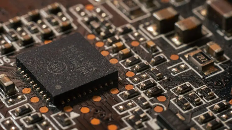
Three wafer categories carry almost all the 2026-2030 volume growth, and they have almost nothing in common on price, spec, or supply chain. 200mm reclaim serves analog, MEMS, and trailing-edge logic; 300mm prime feeds AI accelerators, HBM stack-die, and CPU/GPU; 300mm SOI plus silicon photonics wafers underwrite the optical transceiver and co-packaged optics ramp into 2028-2030 [S2][S3].
Reclaim capacity (150mm, 200mm, 300mm segments) is sized by Grand View Research for the 2025-2030 window as the swing supply for non-leading-edge fabs, with North America and Asia Pacific the dominant regional demand pools [S2]. Monocrystalline wafer list prices on Asian B2B portals sit broadly in the US$10-100 per-piece band at 25-piece MOQ for the entry-level substrate category, with prime 300mm pricing multiples above that band in direct OEM contracts [S1].
Demand engine #1: 200mm and 300mm reclaim for trailing-edge fabs
Reclaim wafers are the recycled monitor and test wafers that every fab burns through, and the segment is segmented by Grand View Research into 150mm, 200mm, and 300mm diameter classes, with integrated circuits and solar panels as the two end-use buckets [S2]. 200mm reclaim remains the volume workhorse because most analog, power discretes, MEMS, and automotive MCUs still run on 200mm lines that are economically irrational to migrate.
Buyers in 2026 should treat reclaim vendors as a strategic, not residual, supply line, especially for the 200mm and 300mm nodes where reclaim polish and particle specs are now within 5-10% of prime on most SEMI standards. The reclaim segment also absorbs cyclical volatility, since solar-panel-grade reclaim can be re-routed when IC demand softens [S2].
For a process engineer building a 2026-2028 capex case, the math is: lock 2-3 qualified reclaim vendors per diameter, hold a 60-90 day safety stock, and audit particle adders per cycle. This is the same playbook the engineering plastics medical device grade map uses for qualified-supplier redundancy in regulated lines.
Demand engine #2: 300mm prime for AI, HBM, and high-performance compute
AI accelerator and HBM stack demand is the single largest pull on 300mm prime wafers through 2030. Each HBM4 stack needs 8-12 DRAM die on a 300mm wafer, and every accelerator package co-packages logic and memory dies, multiplying wafer-area per system sold. The 1.6T optical transceiver commercialization in 2026 is the other pull on 300mm silicon, since silicon photonic modulators, waveguides, and Ge photodetectors all sit on 300mm SOI or bulk silicon [S3].
IDTechEx flags the data-center interconnect bottleneck, where accelerator silicon idles waiting for copper bandwidth, as the structural driver pushing the industry toward 1.6T transceivers in 2026 and 3.2T transceivers toward the end of the decade [S3]. Each 1.6T optical engine uses 2-4 silicon photonic chips per side plus the laser assembly, so the silicon area pulled by optics scales non-linearly with data rate.
For comparison, a hyperscaler buying 100,000 1.6T transceivers in 2026 effectively pulls 200,000-400,000 silicon photonic die, each on a 300mm wafer, on top of the conventional logic and memory wafer demand. Co-packaged optics (CPO) platforms like TSMC COUPE compound this by bringing the optical engine onto the same substrate as the ASIC, which tightens the laser-thermal problem and pushes the photonics wafer spec toward thinner, more planar substrates [S3].
Demand engine #3: silicon photonics and SOI as a separate 300mm niche

Silicon photonics is not a 300mm-prime substitute; it is a parallel 300mm market with its own wafer spec. Photonic Integrated Circuits (PICs) need low-loss waveguides, high-index contrast, and often a buried oxide layer (SOI) to confine light, which is why most PICs ship on 200mm or 300mm SOI rather than bulk prime wafers [S3].
The material-platform split is real: silicon and silica-based PICs dominate light propagation, but silicon's indirect bandgap means a pure silicon laser is physically impossible, so InP, TFLN, and other compound platforms are integrated as light sources and modulators alongside the silicon photonics die [S3]. This makes a 2026-2030 silicon-photonic wafer forecast contingent on the InP and TFLN supply chain, not just silicon.
On the demand side, the 1.6T and 3.2T transceiver roadmap plus CPO adoption into 2028-2030 implies silicon photonic wafer volume growing faster than overall 300mm prime, but from a smaller base. A reasonable working assumption for a procurement plan is that photonic-grade 300mm SOI demand roughly doubles by 2028 against the 2026 baseline, dominated by data-center transceiver and AI accelerator use cases [S3].
Comparison: three wafer types on the 2026-2030 decision grid
The three wafer categories line up against four decision criteria. On price, 200mm reclaim is the cheapest at low double-digit US dollars per piece, monocrystalline entry wafers sit in the US$10-100 per-piece band, and 300mm prime plus SOI for photonics is multiples higher in direct OEM contracts [S1]. On end use, 200mm reclaim feeds analog/MEMS/automotive, 300mm prime feeds logic/HBM, and 300mm SOI plus bulk photonic wafers feed transceivers and CPO [S2][S3].
On supply tightness in 2026, reclaim is the loosest of the three because qualified vendors are growing and 150mm/200mm capacity has a longer history, while 300mm prime is the tightest because AI/HBM demand is absorbing every qualified fab, and 300mm SOI for photonics sits in between, with the binding constraint being the InP and TFLN light-source supply chain rather than the silicon itself [S2][S3]. On risk, reclaim is lowest because it is a recycled, multi-vendor commodity; 300mm prime is highest because it concentrates on a small number of qualified merchant and captive fabs; photonics is highest for technical risk because CPO thermal integration and laser integration are still in active commercialization [S3].
Standards, specs, and what to pin in a 2026 RFQ

Reclaim wafer specs should reference the SEMI M1 (prime wafer geometry) and SEMI HD3 (defect and particle) series for monitor wafer acceptance, with vendor-specific polish and metallic contamination limits, since reclaim is judged on adders per reclaim cycle rather than absolute defect density. For 300mm prime, SEMI M1 plus the SEMI 44-series for flatness and edge profile are the working references, with HBM customer fabs typically demanding sub-50nm nanotopography on the higher-tier SKUs. [S2]
Silicon photonics RFQs need a different spec stack: 200mm or 300mm SOI with a defined buried-oxide thickness (commonly 2-3 micrometers for datacom wavelengths), a silicon device layer in the 200-300 nanometer band, and a waveguide loss budget under 3 dB/cm for the 1310 and 1550 nanometer windows [S3]. Co-packaged optics builds add thermal interface and laser-integration constraints that the wafer spec alone cannot capture, so the RFQ should call out the planned package architecture (TSMC COUPE-style, or a custom organic substrate) and the laser source separately.
For procurement, the rule of thumb is: qualify 2-3 vendors per diameter and per platform (prime vs SOI vs reclaim), audit them on particle and metallic adders per cycle, and do not mix prime and reclaim suppliers on the same tool class without a re-qualification run, because native oxide thickness and surface microroughness drift between vendors even within spec. This is the same risk-management logic that face shield selection for confined space entry applies to multi-vendor PPE, where a spec-compliant alternate can still fail a fit or chemical compatibility test.
Limits, failure modes, and what the 2026-2030 forecast cannot tell you
Three failure modes sit on top of the demand picture. First, reclaim cycles accumulate subsurface damage; a reclaim wafer reused past 4-6 cycles typically loses flatness and particle spec, so the 2026-2030 forecast assumes a steady mix of new prime and reclaim, not a pure reclaim substitution. Second, 300mm prime supply is concentrated, and a single qualified-fab outage tightens the whole market for 6-9 months, which is why hyperscalers lock 12-24 month wafer supply contracts. [S2]
Third, silicon photonics is gated by laser integration and packaging, not by silicon wafer volume, so a 1.6T and 3.2T transceiver ramp can be demand-limited by InP and TFLN supply, not by silicon. IDTechEx notes that silicon is an indirect bandgap material, which means pure silicon lasers are impossible, forcing hybrid integration of III-V or TFLN light sources on the silicon photonics die [S3]. This means a wafer buyer who locks silicon photonic supply without locking the light-source supply is exposed to a different bottleneck downstream.
For an engineer building a 2026-2030 capacity plan, the practical filter is: confirm reclaim supply for trailing-edge lines by end of 2026, commit to multi-year 300mm prime contracts for AI/HBM wafer demand, and treat silicon photonic wafer demand as a co-dependent bet on CPO and 3.2T transceiver commercialization, not as a stand-alone silicon volume forecast [S3]. The next verifiable signal to watch is 3.2T transceiver volume shipments in 2028, and the second is reclaim vendor capacity announcements for 300mm in North America through 2027 [S2][S3].
Spec-level background on the components involved: silicon carbide, silicon nitride, and silicon steel.